RXENA
RXRDY
1
6
3 4
52
0 1 2 3 4 5 0 1 2
Start Stop StartAd Pa
SCIRXDpin
Frame
Majority
vote
Startbit LSBofdata
SCICLK
(internal)
SCIRXD
1 2 3 4 5 6 7 8 1 2 3 4 5 6 7 8 1
8SCICLKperiodsperdatabit 8SCICLKperiodsperdatabit
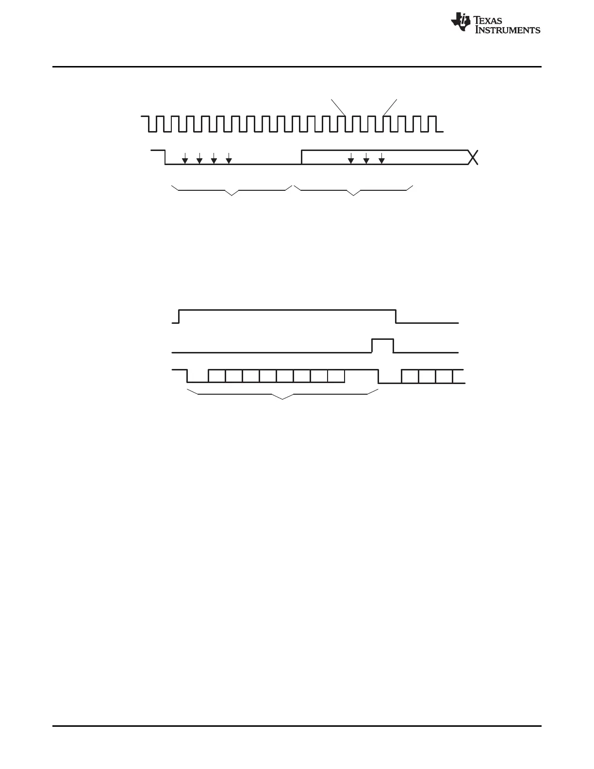
SCI Communication Format
www.ti.com
590
SPRUI07–March 2020
Submit Documentation Feedback
Copyright © 2020, Texas Instruments Incorporated
Serial Communications Interface (SCI)
Figure 10-7. SCI Asynchronous Communications Format
10.10.1 Receiver Signals in Communication Modes
Figure 10-8 illustrates an example of receiver signal timing that assumes the following conditions:
• Address-bit wake-up mode (address bit does not appear in idle-line mode)
• Six bits per character
Figure 10-8. SCI RX Signals in Communication Modes
(1) Data arrives on the SCIRXD pin, start bit detected.
(2) Bit RXENA is brought low to disable the receiver. Data continues to be assembled in RXSHF but is not
transferred to the receiver buffer register.
Notes:
1. Flag bit RXENA (SCICTL1, bit 0) goes high to enable the receiver.
2. Data arrives on the SCIRXD pin, start bit detected.
3. Data is shifted from RXSHF to the receiver buffer register (SCIRXBUF); an interrupt is requested. Flag
bit RXRDY (SCIRXST, bit 6) goes high to signal that a new character has been received.
4. The program reads SCIRXBUF; flag RXRDY is automatically cleared.
5. The next byte of data arrives on the SCIRXD pin; the start bit is detected, then cleared.
6. Bit RXENA is brought low to disable the receiver. Data continues to be assembled in RXSHF but is not
transferred to the receiver buffer register.
10.10.2 Transmitter Signals in Communication Modes
Figure 10-9 illustrates an example of transmitter signal timing that assumes the following conditions:
• Address-bit wake-up mode (address bit does not appear in idle-line mode)
• Three bits per character
 Loading...