FSG
CLKG
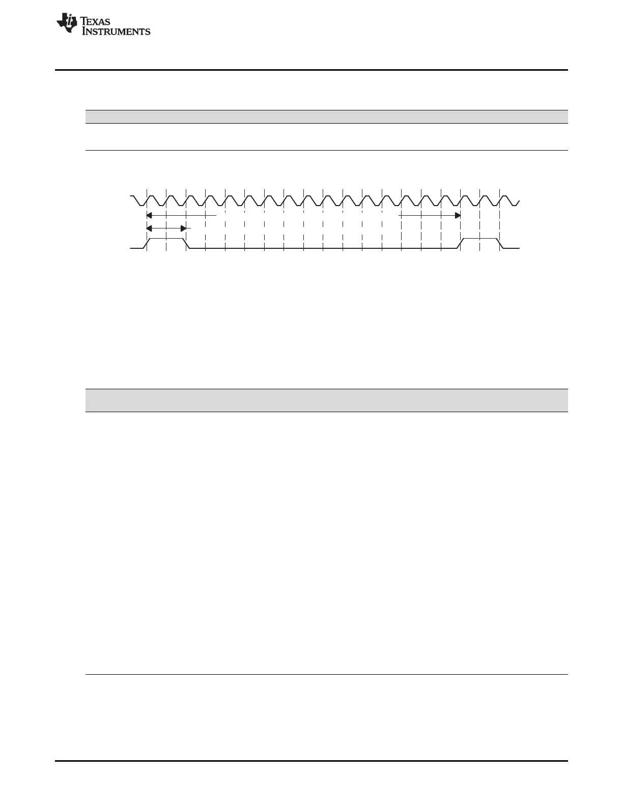
19181716151413121110987654321
Frame-synchronization pulse width: (FWID + 1) x CLKG
Frame-synchronization period: (FPER+1) x CLKG
www.ti.com
Receiver Configuration
713
SPRUI07–March 2020
Submit Documentation Feedback
Copyright © 2020, Texas Instruments Incorporated
Multichannel Buffered Serial Port (McBSP)
Table 12-39. Register Bits Used to Set the SRG Frame-Synchronization Period and Pulse
Width (continued)
Register Bit Name Function Type Reset Value
Range for (FWID + 1):
1 to 256 CLKG cycles
Figure 12-49. Frame of Period 16 CLKG Periods and Active Width of 2 CLKG Periods
When the sample rate generator comes out of reset, FSG is in its inactive state. Then, when GRST = 1
and FSGM = 1, a frame-synchronization pulse is generated. The frame width value (FWID + 1) is counted
down on every CLKG cycle until it reaches 0, at which time FSG goes low. At the same time, the frame
period value (FPER + 1) is also counting down. When this value reaches 0, FSG goes high, indicating a
new frame.
12.8.17 Receive Clock Mode
Table 12-40 shows the settings for bits used to set receive clock mode.
Table 12-40. Register Bits Used to Set the Receive Clock Mode
Register Bit Name Function Type
Reset
Value
PCR 8 CLKRM Receive clock mode R/W 0
Case 1: Digital loopback mode not set (DLB = 0) in SPCR1.
CLKRM = 0 The MCLKR pin is an input pin that supplies the
internal receive clock (MCLKR).
CLKRM = 1 Internal MCLKR is driven by the sample rate
generator of the McBSP. The MCLKR pin is an
output pin that reflects internal MCLKR.
Case 2: Digital loopback mode set (DLB = 1) in SPCR1.
CLKRM = 0 The MCLKR pin is in the high impedance state.
The internal receive clock (MCLKR) is driven by
the internal transmit clock (CLKX). Internal
CLKX is derived according to the CLKXM bit of
PCR.
CLKRM = 1 Internal MCLKR is driven by internal CLKX. The
MCLKR pin is an output pin that reflects internal
MCLKR. Internal CLKX is derived according to
the CLKXM bit of PCR.
SPCR1 15 DLB Digital loopback mode R/W 00
DLB = 0 Digital loopback mode is disabled.
DLB = 1 Digital loopback mode is enabled. The receive
signals, including the receive frame-
synchronization signal, are connected internally
through multiplexers to the corresponding
transmit signals.
 Loading...