ac
R
s
ADCIN0
C
p
10 pF
R
on
1 kΩ
1.64 pF
C
h
Switch
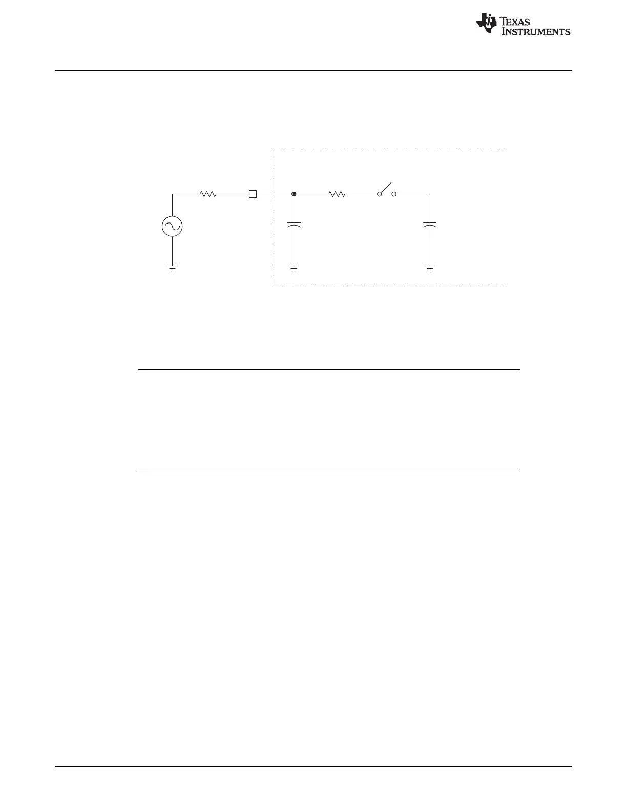
Typical Values of the Input Circuit Components:
Switch Resistance (R
on
): 1 kΩ
Sampling Capacitor (C
h
): 1.64 pF
Parasitic Capacitance (C
p
): 10 pF
Source Resistance (R
s
): 50 Ω
28x DSP
Source
Signal
ADC Circuit
www.ti.com
450
SPRUI07–March 2020
Submit Documentation Feedback
Copyright © 2020, Texas Instruments Incorporated
Analog-to-Digital Converter (ADC)
7.2.2 ADC Sample and Hold Circuit and Modeling
As shown in Figure 7-4 , the ADCIN pins can be modeled as an RC circuit. With VREFLO connected to
ground, a voltage swing from 0 to 3.3v on ADCIN yields a typical RC time constant of 2ns.
Figure 7-4. ADCINx Input Model
NOTE: The ADC does not precondition the Ch capacitor voltage before conversions, therefore the
following behaviors apply:
1. There is no predetermined ADC conversion value when the ADCIN pin is not
connected to a Source Signal
2. Residual charge will remain on Ch between ADC conversions
3. Sequential conversions may suffer from cross-talk if the ACQPS window is too
short for Ch to settle
For correct operation, the input signal to the ADC must be allowed adequate time to charge the sample
and hold capacitor, C
h
. Typically, the S+H duration is chosen such that C
h
will be charged to within ½ LSB
or ¼ LSB of the final value, depending on the tolerable settling error.
The S+H time required to satisfy the settling error is largely influenced by the bandwidth of the source
signal. Therefore, the following recommendations for approximating the S+H duration will be simplified into
two practical scenarios of either high bandwidth or low bandwidth signals. A high bandwidth source signal
will be characterized as being able to meet the settling error and real-time requirements of the system
using a supported ACQPS setting. A low bandwidth source signal is one that requires a longer S+H
duration than is acceptable.
 Loading...