MAX CONV1
Ch Sel (CONV00)
Ch Sel (CONV01)
Ch Sel (CONV03)
Ch Sel (CONV02)
Ch Sel (CONV07)
State
pointer
12-bit
A/D
converter
EOC
12
Result MUX
Result
select
12
SEQ1
Software
ePWMx SOCA
External pin
(XINT2_ADCSOC)
Note: Possible values:
Channel select = 0 to 15
MAX CONV1 = 0 to 7
SOC1 EOC1
MUX
Ch Sel (CONV15)
Ch Sel (CONV08)
Ch Sel (CONV09)
Ch Sel (CONV11)
Ch Sel (CONV10)
ePWMx SOCB
MAX CONV2
SOC2
EOC2
4
Software
SEQ2
Start-of-sequence
trigger
Result
select
12
Result MUX
12
12
MAX CONV2 = 0 to 7
State
pointer
Start-of-sequence
trigger
4
4 4
SOC
Sequencer arbiter
ADCINA0
ADCINA1
ADCINA7
Analog MUX
MUX
select
ADCINB1
ADCINB7
MUX
select
ADCINB0
S/H-A
S/H-B
ADC start of conversion (SOC) trigger sources
ADCRESULT0
ADCRESULT1
ADCRESULT7
ADCRESULT8
ADCRESULT9
ADCRESULT15
ADC Interface
www.ti.com
464
SPRUI07–March 2020
Submit Documentation Feedback
Copyright © 2020, Texas Instruments Incorporated
Analog-to-Digital Converter (ADC)
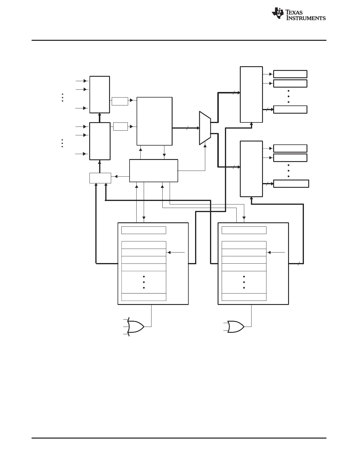
Figure 7-9. Block Diagram of Autosequenced ADC With Dual Sequencers
NOTE: There is only one ADC in the DSP. This converter is shared by the two sequencers in dual-sequencer mode.
 Loading...