ADC Registers
www.ti.com
490
SPRUI07–March 2020
Submit Documentation Feedback
Copyright © 2020, Texas Instruments Incorporated
Analog-to-Digital Converter (ADC)
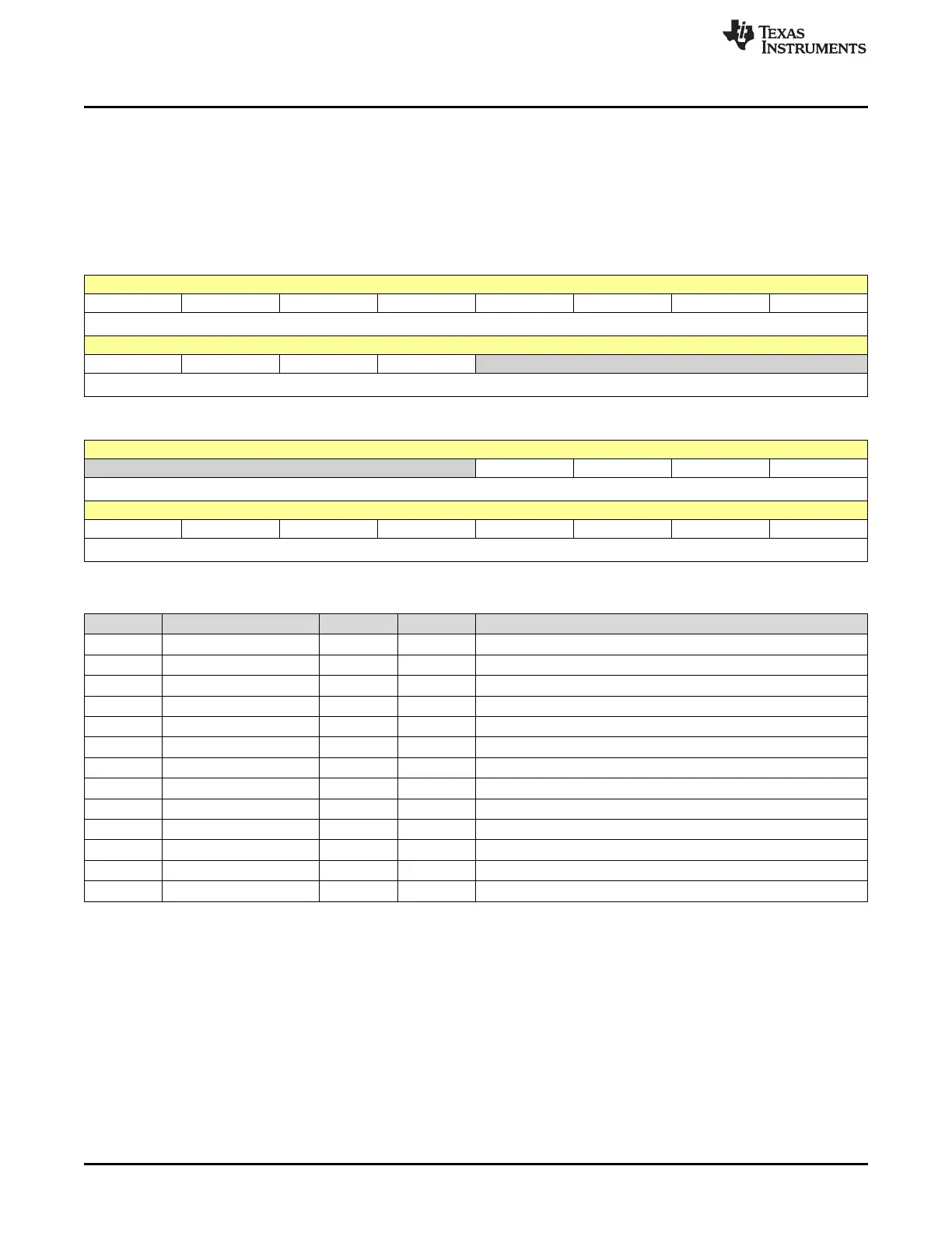
7.4.9 ADCRESULT_0 to ADCRESULT_15 Register (Offset = 8h to 17h) [reset = 0h]
ADCRESULT_0 to ADCRESULT_15 is shown in Figure 7-23 and described in Table 7-21.
In the cascaded sequencer mode, registers ADCRESULT8 through ADCRESULT15 holds the results of
the ninth through sixteenth conversions. The ADCRESULTn registers are left justified when read from
Peripheral Frame 2 (0x7108-0x7117) with two wait states and right justified when read from the mirror
registers in Peripheral Frame 0 (0x0B00-0x0B0F) with zero wait states.
Figure 7-23. ADCRESULT_0 to ADCRESULT_15 Register
15 14 13 12 11 10 9 8
D11 D10 D9 D8 D7 D6 D5 D4
R-0h R-0h R-0h R-0h R-0h R-0h R-0h R-0h
7 6 5 4 3 2 1 0
D3 D2 D1 D0 RESERVED
R-0h R-0h R-0h R-0h R-0h
Figure 7-24. ADCRESULT_0 to ADCRESULT_15 Register (Addresses 0x0B00-0x0B0F)
15 14 13 12 11 10 9 8
RESERVED D11 D10 D9 D8
R-0h R-0h R-0h R-0h R-0h
7 6 5 4 3 2 1 0
D7 D6 D5 D4 D3 D2 D1 D0
R-0h R-0h R-0h R-0h R-0h R-0h R-0h R-0h
Table 7-21. ADCRESULT_0 to ADCRESULT_15 Register Field Descriptions
Bit Field Type Reset Description
15 D11 R 0h
14 D10 R 0h
13 D9 R 0h
12 D8 R 0h
11 D7 R 0h
10 D6 R 0h
9 D5 R 0h
8 D4 R 0h
7 D3 R 0h
6 D2 R 0h
5 D1 R 0h
4 D0 R 0h
3-0 RESERVED R 0h
 Loading...