McBSP Registers
www.ti.com
748
SPRUI07–March 2020
Submit Documentation Feedback
Copyright © 2020, Texas Instruments Incorporated
Multichannel Buffered Serial Port (McBSP)
12.15.3.1 Data Travel From Registers to Data Transmit (DX) Pins
If the serial word length is 16 bits or fewer, data written to DXR1 is copied to transmit shift register 1
(XSR1). From XSR1, the data is shifted onto the DX pin one bit at a time. The XSRs are not accessible.
If the serial word length is more than 16 bits, data written to DXR1 and DXR2 is copied to both transmit
shift registers (XSR2, XSR1). From the XSRs, the data is shifted onto the DX pin one bit at a time.
If companding is used during the transfer from DXR1 to XSR1 (XCOMPAND = 10b or 11b), the McBSP
compresses the 16-bit data in DXR1 to 8-bit data in the μ-law or A-law format in XSR1. If companding is
disabled, the McBSP passes data from the DXR(s) to the XSR(s) without modification.
12.15.4 Serial Port Control Registers (SPCR[1,2])
Each McBSP has two serial port control registers, SPCR1 (Table 12-77) and SPCR2 (Table 12-78). These
registers enable you to:
• Control various McBSP modes: digital loopback mode (DLB), sign-extension and justification mode for
reception (RJUST), clock stop mode (CLKSTP), interrupt modes (RINTM and XINTM), emulation mode
(FREE and SOFT)
• Turn on and off the DX-pin delay enabler (DXENA)
• Check the status of receive and transmit operations (RSYNCERR, XSYNCERR, RFULL, XEMPTY,
RRDY, XRDY)
• Reset portions of the McBSP (RRST, XRST, FRST, GRST)
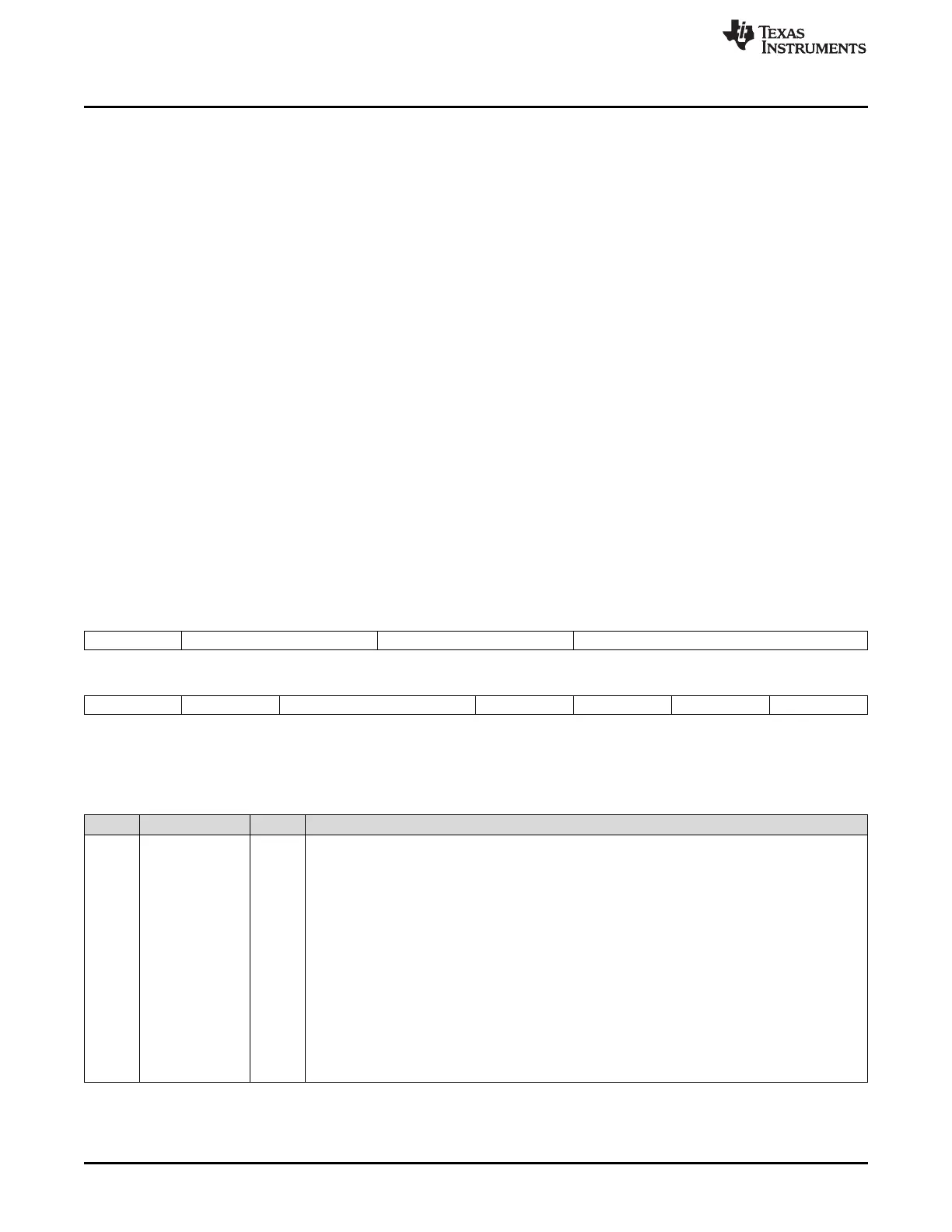
12.15.4.1 Serial Port Control 1 Register (SPCR1)
The serial port control 1 register (SPCR1) is shown in Figure 12-69 and described in Table 12-77.
Figure 12-69. Serial Port Control 1 Register (SPCR1)
15 14 13 12 11 10 8
DLB RJUST CLKSTP Reserved
R/W-0 R/W-0 R/W-0 R-0
7 6 5 4 3 2 1 0
DXENA Reserved RINTM RSYNCERR RFULL RRDY RRST
R/W-0 R/W-0 R/W-0 R/W-0 R-0 R-0 R/W-0
LEGEND: R/W = Read/Write; R = Read only; -n = value after reset
Table 12-77. Serial Port Control 1 Register (SPCR1) Field Descriptions
Bit Field Value Description
15 DLB Digital loopback mode bit. DLB disables or enables the digital loopback mode of the McBSP:
0 Disabled
Internal DR is supplied by the MDRx pin. Internal FSR and internal MCLKR can be supplied by their
respective pins or by the sample rate generator, depending on the mode bits FSRM and CLKRM.
Internal DX is supplied by the MDXx pin. Internal FSX and internal CLKX are supplied by their
respective pins or are generated internally, depending on the mode bits FSXM and CLKXM.
1 Enabled
Internal receive signals are supplied by internal transmit signals:
MDRx connected to MDXx
MFSRx connected to MFSXx
MCLKR connected to MCLKXx
This mode allows you to test serial port code with a single DSP. The McBSP transmitter directly
supplies data, frame synchronization, and clocking to the McBSP receiver.
 Loading...