General-Purpose Input/Output (GPIO)
www.ti.com
122
SPRUI07–March 2020
Submit Documentation Feedback
Copyright © 2020, Texas Instruments Incorporated
System Control and Interrupts
Typically the DAT registers are used for reading the current state of the pins. To easily modify the output
level of the pin refer to the SET, CLEAR and TOGGLE registers.
(1)
x = The state of the GPADAT register is unknown after reset. It depends on the level of the pin after reset.
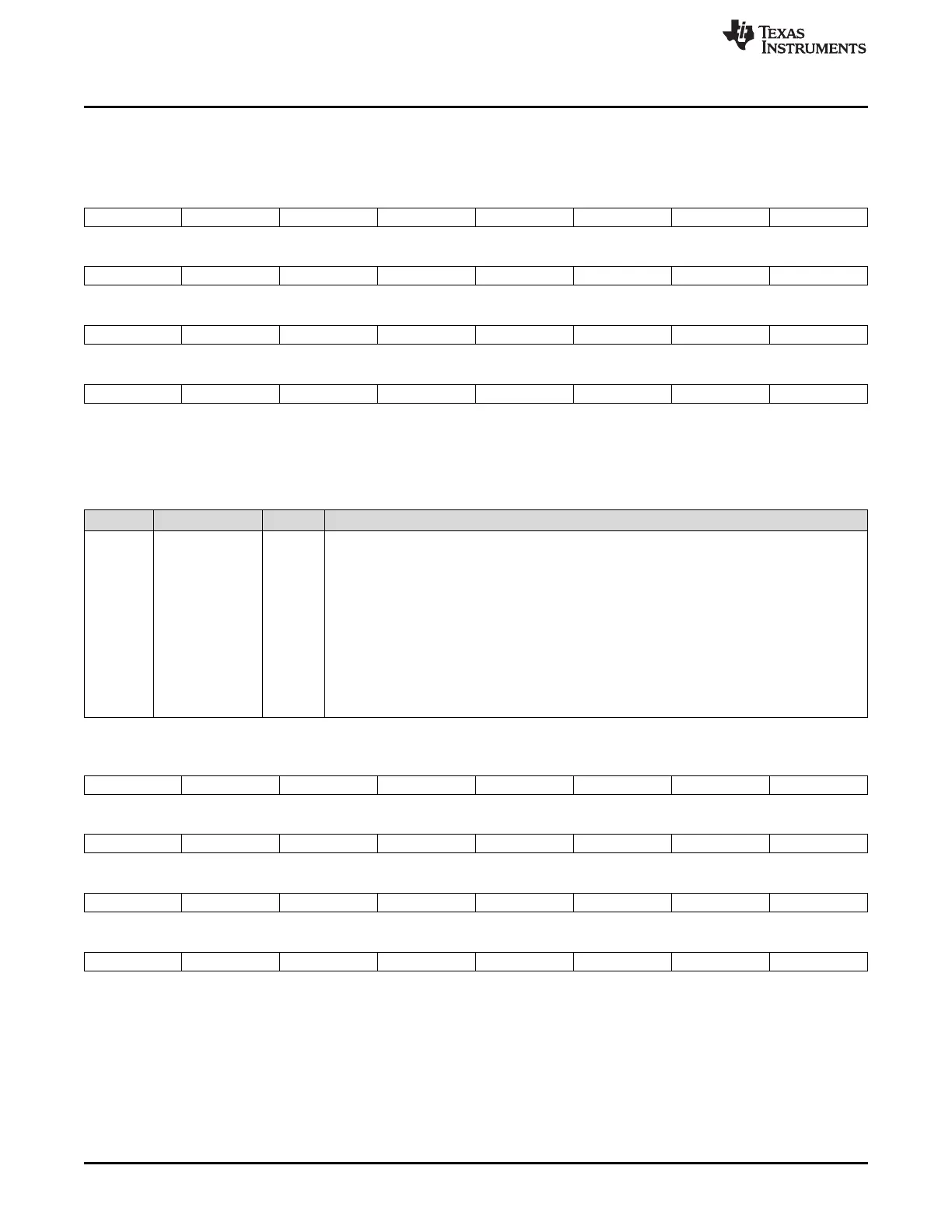
Figure 1-65. GPIO Port A Data (GPADAT) Register
31 30 29 28 27 26 25 24
GPIO31 GPIO30 GPIO29 GPIO28 GPIO27 GPIO26 GPIO25 GPIO24
R/W-x R/W-x R/W-x R/W-x R/W-x R/W-x R/W-x R/W-x
23 22 21 20 19 18 17 16
GPIO23 GPIO22 GPIO21 GPIO20 GPIO19 GPIO18 GPIO17 GPIO16
R/W-x R/W-x R/W-x R/W-x R/W-x R/W-x R/W-x R/W-x
15 14 13 12 11 10 9 8
GPIO15 GPIO14 GPIO13 GPIO12 GPIO11 GPIO10 GPIO9 GPIO8
R/W-x R/W-x R/W-x R/W-x R/W-x R/W-x R/W-x R/W-x
7 6 5 4 3 2 1 0
GPIO7 GPIO6 GPIO5 GPIO4 GPIO3 GPIO2 GPIO1 GPIO0
R/W-x R/W-x R/W-x R/W-x R/W-x R/W-x R/W-x R/W-x
LEGEND: R/W = Read/Write; R = Read only; -n = value after reset
(1)
Table 1-68. GPIO Port A Data (GPADAT) Register Field Descriptions
Bits Field Value Description
31-0 GPIO31-GPIO0 Each bit corresponds to one GPIO port A pin (GPIO0-GPIO31) as shown in Figure 1-65.
0 Reading a 0 indicates that the state of the pin is currently low, irrespective of the mode the pin is
configured for.
Writing a 0 will force an output of 0 if the pin is configured as a GPIO output in the appropriate
GPAMUX1/2 and GPADIR registers; otherwise, the value is latched but not used to drive the
pin.
1 Reading a 1 indicates that the state of the pin is currently high irrespective of the mode the pin
is configured for.
Writing a 1will force an output of 1if the pin is configured as a GPIO output in the appropriate
GPAMUX1/2 and GPADIR registers; otherwise, the value is latched but not used to drive the
pin.
(1)
x = The state of the GPADAT register is unknown after reset. It depends on the level of the pin after reset.
Figure 1-66. GPIO Port B Data (GPBDAT) Register
31 30 29 28 27 26 25 24
GPIO63 GPIO62 GPIO61 GPIO60 GPIO59 GPIO58 GPIO57 GPIO56
R/W-x R/W-x R/W-x R/W-x R/W-x R/W-x R/W-x R/W-x
23 22 21 20 19 18 17 16
GPIO55 GPIO54 GPIO53 GPIO52 GPIO51 GPIO50 GPIO49 GPIO48
R/W-x R/W-x R/W-x R/W-x R/W-x R/W-x R/W-x R/W-x
15 14 13 12 11 10 9 8
GPIO47 GPIO46 GPIO45 GPIO44 GPIO43 GPIO42 GPIO41 GPIO40
R/W-x R/W-x R/W-x R/W-x R/W-x R/W-x R/W-x R/W-x
7 6 5 4 3 2 1 0
GPIO39 GPIO38 GPIO37 GPIO36 GPIO35 GPIO34 GPIO33 GPIO32
R/W-x R/W-x R/W-x R/W-x R/W-x R/W-x R/W-x R/W-x
LEGEND: R/W = Read/Write; R = Read only; -n = value after reset
(1)
 Loading...