Receiver Configuration
www.ti.com
712
SPRUI07–March 2020
Submit Documentation Feedback
Copyright © 2020, Texas Instruments Incorporated
Multichannel Buffered Serial Port (McBSP)
Similarly, the receiver can reliably sample data that is clocked with a rising edge clock (by the transmitter).
The receive clock polarity bit, CLKRP, sets the edge used to sample received data. The receive data is
always sampled on the falling edge of internal MCLKR. Therefore, if CLKRP = 1 and external clocking is
selected (CLKRM = 0 and MCLKR is an input pin), the external rising-edge triggered input clock on
MCLKR is inverted to a falling-edge triggered clock before being sent to the receiver. If CLKRP = 1 and
internal clocking is selected (CLKRM = 1), the internal falling-edge triggered clock is inverted to a rising-
edge triggered clock before being sent out on the MCLKR pin.
MCLKRP = CLKXP in a system where the same clock (internal or external) is used to clock the receiver
and transmitter. The receiver uses the opposite edge as the transmitter to ensure valid setup and hold of
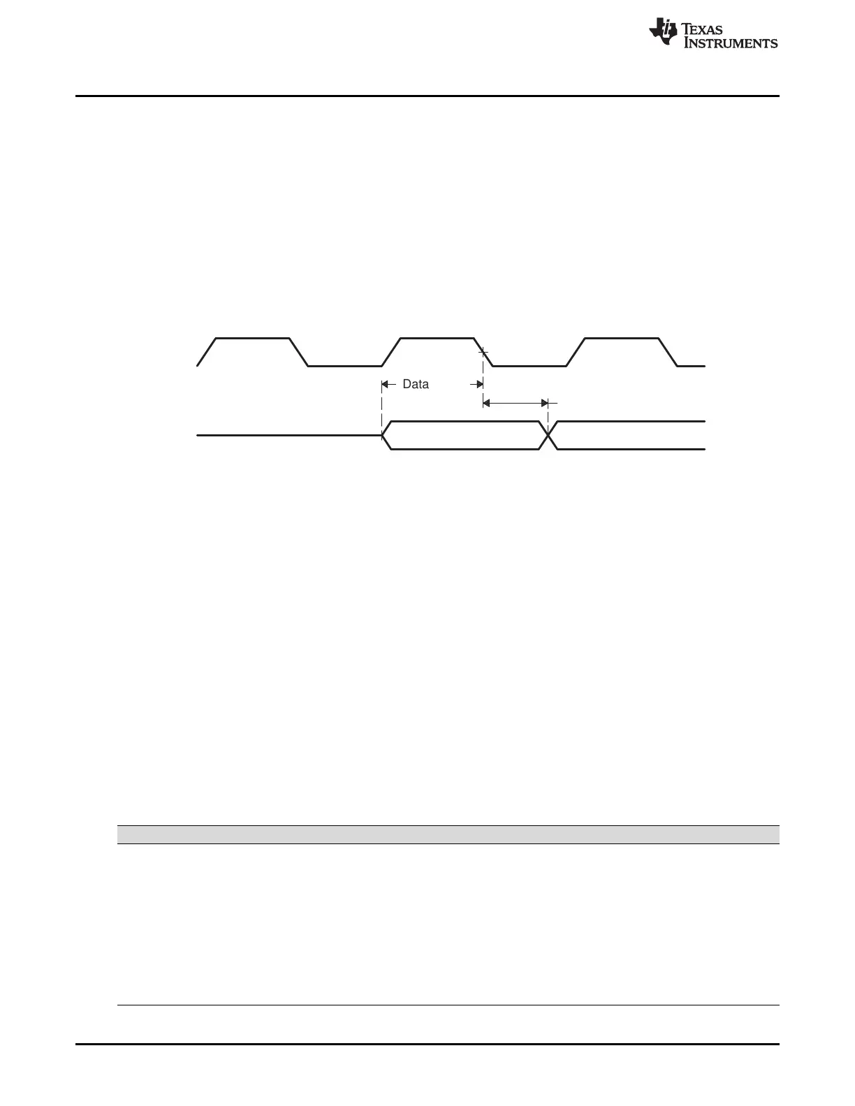
data around this edge. Figure 12-48 shows how data clocked by an external serial device using a rising
edge can be sampled by the McBSP receiver on the falling edge of the same clock.
Figure 12-48. Data Clocked Externally Using a Rising Edge and Sampled by the McBSP Receiver on a
Falling Edge
Set the SRG Frame-Synchronization Period and Pulse Width
12.8.16.2 Frame-Synchronization Period and the Frame-Synchronization Pulse Width
The sample rate generator can produce a clock signal, CLKG, and a frame-synchronization signal, FSG. If
the sample rate generator is supplying receive or transmit frame synchronization, you must program the
bit fields FPER and FWID.
On FSG, the period from the start of a frame-synchronization pulse to the start of the next pulse is (FPER
+ 1) CLKG cycles. The 12 bits of FPER allow a frame-synchronization period of 1 to 4096 CLKG cycles,
which allows up to 4096 data bits per frame. When GSYNC = 1, FPER is a don't care value.
Each pulse on FSG has a width of (FWID + 1) CLKG cycles. The eight bits of FWID allow a pulse width of
1 to 256 CLKG cycles. It is recommended that FWID be programmed to a value less than the
programmed word length.
The values in FPER and FWID are loaded into separate down-counters. The 12-bit FPER counter counts
down the generated clock cycles from the programmed value (4095 maximum) to 0. The 8-bit FWID
counter counts down from the programmed value (255 maximum) to 0. Table 12-39 shows settings for
FPER and FWID.
Figure 12-49 shows a frame-synchronization period of 16 CLKG periods (FPER = 15 or 00001111b) and a
frame-synchronization pulse with an active width of 2 CLKG periods (FWID = 1).
Table 12-39. Register Bits Used to Set the SRG Frame-Synchronization Period and Pulse Width
Register Bit Name Function Type Reset Value
SRGR2 11-0 FPER Sample rate generator frame-synchronization period R/W 0000 0000 0000
For the frame-synchronization signal FSG, (FPER + 1)
determines the period from the start of a frame-
synchronization pulse to the start of the next frame-
synchronization pulse.
Range for (FPER + 1):
1 to 4096 CLKG cycles
SRGR1 15-8 FWID Sample rate generator frame-synchronization pulse width R/W 0000 0000
This field plus 1 determines the width of each frame-
synchronization pulse on FSG.
 Loading...