General-Purpose Input/Output (GPIO)
www.ti.com
126
SPRUI07–March 2020
Submit Documentation Feedback
Copyright © 2020, Texas Instruments Incorporated
System Control and Interrupts
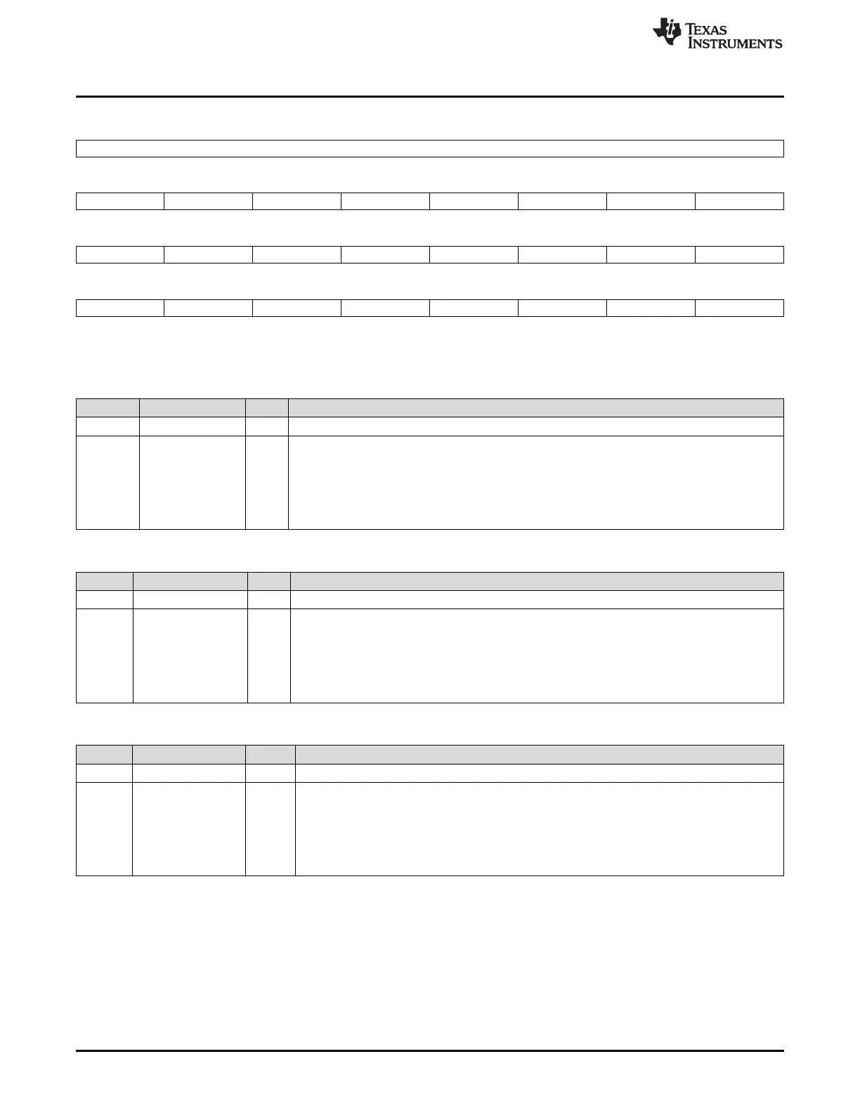
Figure 1-70. GPIO Port C Set, Clear and Toggle (GPCSET, GPCCLEAR, GPCTOGGLE) Registers
31 24
Reserved
R-0
23 22 21 20 19 18 17 16
GPIO87 GPIO86 GPIO85 GPIO84 GPIO83 GPIO82 GPIO81 GPIO80
R/W-0 R/W-0 R/W-0 R/W-0 R/W-0 R/W-0 R/W-0 R/W-0
15 14 13 12 11 10 9 8
GPIO79 GPIO78 GPIO77 GPIO76 GPIO75 GPIO74 GPIO73 GPIO72
R/W-0 R/W-0 R/W-0 R/W-0 R/W-0 R/W-0 R/W-0 R/W-0
7 6 5 4 3 2 1 0
GPIO71 GPIO70 GPIO69 GPIO68 GPIO67 GPIO66 GPIO65 GPIO64
R/W-0 R/W-0 R/W-0 R/W-0 R/W-0 R/W-0 R/W-0 R/W-0
LEGEND: R/W = Read/Write; R = Read only; -n = value after reset
Table 1-77. GPIO Port C Set (GPCSET) Register Field Descriptions
Bits Field Value Description
31-24 Reserved Reserved
23-0 GPIO87-GPIO64 Each GPIO port C pin (GPIO64-GPIO87) corresponds to one bit in this register as shown in
Figure 1-70.
0 Writes of 0 are ignored. This register always reads back a 0.
1 Writing a 1 forces the respective output data latch to high. If the pin is configured as a GPIO
output then it will be driven high. If the pin is not configured as a GPIO output then the latch is
set but the pin is not driven.
Table 1-78. GPIO Port C Clear (GPCCLEAR) Register Field Descriptions
Bits Field Value Description
31-24 Reserved Reserved
23-0 GPIO87-GPIO64 Each GPIO port C pin (GPIO64-GPIO87) corresponds to one bit in this register as shown in
Figure 1-70.
0 Writes of 0 are ignored. This register always reads back a 0.
1 Writing a 1 forces the respective output data latch to low. If the pin is configured as a GPIO
output then it will be driven low. If the pin is not configured as a GPIO output then the latch is
cleared but the pin is not driven.
Table 1-79. GPIO Port C Toggle (GPCTOGGLE) Register Field Descriptions
Bits Field Value Description
31-24 Reserved Reserved
23-0 GPIO87-GPIO64 Each GPIO port C pin (GPIO64-GPIO87) corresponds to one bit in this register as shown in
Figure 1-70.
0 Writes of 0 are ignored. This register always reads back a 0.
1 Writing a 1 forces the respective output data latch to toggle from its current state. If the pin is
configured as a GPIO output then it will be driven in the opposite direction of its current state. If
the pin is not configured as a GPIO output then the latch is cleared but the pin is not driven.
 Loading...