MOV
TBIT
@REG1,AL
@REG2,#BIT_X Read
Write
XD(31:0)
XA(19:0)
XZCS0
XZCS6
XZCS7
XWE0
XR/W
XREADY
XHOLD
XHOLDA
XCLKOUT
XRD
XINTFZone0
(8Kx16)
XINTFZone7
(1Mx16)
0x0030−0000
0x0020−0000
0x0010−0000
0x0000−5000
0x0000−4000
0x0000−0000
DataSpace ProgSpace
XINTFZone6
(1Mx16)
XA0/XWE1
www.ti.com
Functional Description
837
SPRUI07–March 2020
Submit Documentation Feedback
Copyright © 2020, Texas Instruments Incorporated
External Interface (XINTF)
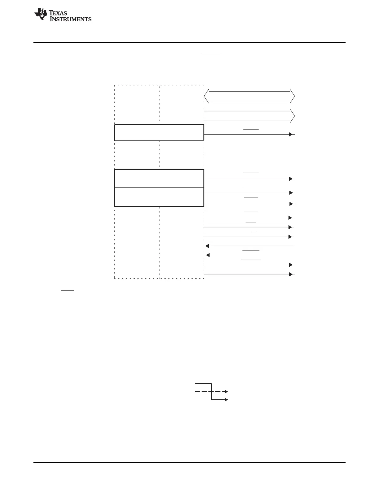
• Zone 6 and 7 both use external addresses 0x00000 - 0xFFFFF. Depending on which zone is
accessed, the appropriate zone chip select signal (XZCS6 or XZCS7) will also go low.
Figure 14-1. External Interface Block Diagram
A Each zone can be programmed with different wait states, setup and hold timings. A dedicated zone chip select
(XZCS) signal toggles when an access to a particular zone is performed. These features enable glueless connection
to many external memories and peripherals.
B Zones 1 − 5 are reserved for future expansion.
C When the XINTF clock is enabled in PCLKCR3, all zones are enabled.
14.1.4 Write-Followed-by-Read Pipeline Protection
In the 28x CPU pipeline, the read phase of an operation occurs before the write phase. Due to this
ordering, a write followed by a read access can actually occur in the opposite order: read followed by
write.
For example, the following lines of code perform a write to one location followed by a read from another.
Due to the 28x CPU pipeline, the read operation will be issued before the write as shown:
On 28x devices, regions of memory where peripheral registers are common are protected from this order
reversal by hardware. These regions of memory are said to be read-followed-by-write pipeline protected.
XINTF Zone 0 is by default read-followed-by-write pipeline protected. Write and read accesses to Zone 0
are executed in the same order that they are written. For example, a write followed by a read is executed
in the same order it was written as shown below:
 Loading...