SPI Registers
www.ti.com
564
SPRUI07–March 2020
Submit Documentation Feedback
Copyright © 2020, Texas Instruments Incorporated
Serial Peripheral Interface (SPI)
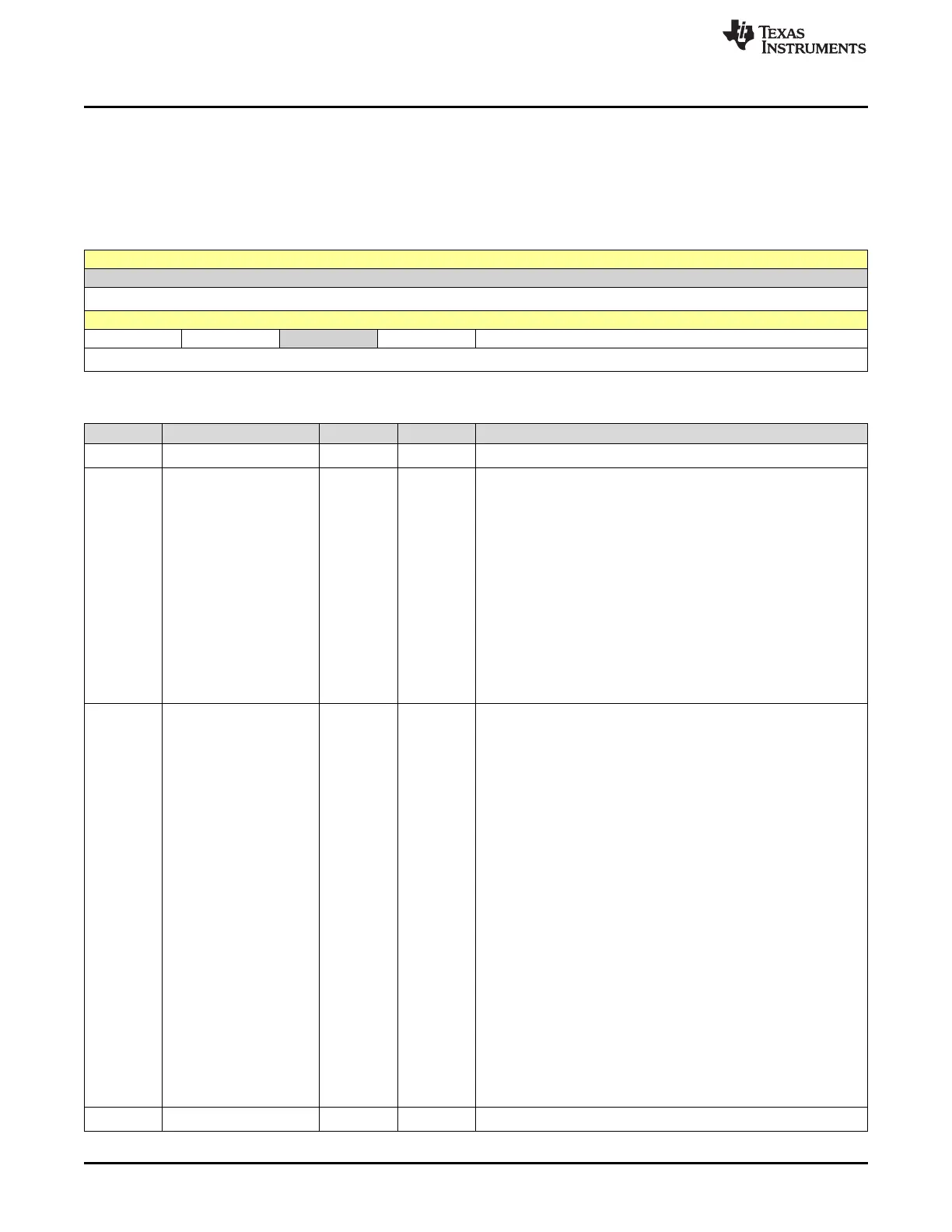
9.5.2.1 SPICCR Register (Offset = 0h) [reset = 0h]
SPICCR is shown in Figure 9-8 and described in Table 9-7.
Return to the Summary Table.
SPICCR controls the setup of the SPI for operation.
Figure 9-8. SPICCR Register
15 14 13 12 11 10 9 8
RESERVED
R-0h
7 6 5 4 3 2 1 0
SPISWRESET CLKPOLARITY RESERVED SPILBK SPICHAR
R/W-0h R/W-0h R-0h R/W-0h R/W-0h
Table 9-7. SPICCR Register Field Descriptions
Bit Field Type Reset Description
15-8 RESERVED R 0h
Reserved
7 SPISWRESET R/W 0h
SPI Software Reset
When changing configuration, you should clear this bit before the
changes and set this bit before resuming operation.
Reset type: SYSRSn
0h (R/W) = Initializes the SPI operating flags to the reset condition.
Specifically, the RECEIVER OVERRUN Flag bit (SPISTS.7), the
SPI INT FLAG bit (SPISTS.6), and the TXBUF FULL Flag bit
(SPISTS.5) are cleared. SPISTE will become inactive. SPICLK will
be immediately driven to 0 regardless of the clock polarity. The SPI
configuration remains unchanged.
1h (R/W) = SPI is ready to transmit or receive the next character.
When the SPI SW RESET bit is a 0, a character written to the
transmitter will not be shifted out when this bit is set. A new
character must be written to the serial data register. SPICLK will be
returned to its inactive state one SPICLK cycle after this bit is set.
6 CLKPOLARITY R/W 0h
Shift Clock Polarity
This bit controls the polarity of the SPICLK signal. CLOCK
POLARITY and POLARITY CLOCK PHASE (SPICTL.3) control four
clocking schemes on the SPICLK pin.
Reset type: SYSRSn
0h (R/W) = Data is output on rising edge and input on falling edge.
When no SPI data is sent, SPICLK is at low level. The data input
and output edges depend on the value of the CLOCK PHASE bit
(SPICTL.3) as follows:
- CLOCK PHASE = 0: Data is output on the rising edge of the
SPICLK signal. Input data is latched on the falling edge of the
SPICLK signal.
- CLOCK PHASE = 1: Data is output one half-cycle before the first
rising edge of the SPICLK signal and on subsequent falling edges
of the SPICLK signal. Input data is latched on the rising edge of
the SPICLK signal.
1h (R/W) = Data is output on falling edge and input on rising edge.
When no SPI data is sent, SPICLK is at high level. The data input
and output edges depend on the value of the CLOCK PHASE bit
(SPICTL.3) as follows:
- CLOCK PHASE = 0: Data is output on the falling edge of the
SPICLK signal. Input data is latched on the rising edge of the
SPICLK signal.
- CLOCK PHASE = 1: Data is output one half-cycle before the first
falling edge of the SPICLK signal and on subsequent rising edges
of the SPICLK signal. Input data is latched on the falling edge of
the SPICLK signal.
5 RESERVED R 0h
Reserved
 Loading...