A1
D(R/X)
FS(R/X)
CLK(R/X)
C5C6C7
B0B1B2B3B4B5B6B7A0
McBSP Operation
www.ti.com
666
SPRUI07–March 2020
Submit Documentation Feedback
Copyright © 2020, Texas Instruments Incorporated
Multichannel Buffered Serial Port (McBSP)
12.3.4 Frame Phases
The McBSP allows you to configure each frame to contain one or two phases. The number of words and
the number of bits per word can be specified differently for each of the two phases of a frame, allowing
greater flexibility in structuring data transfers. For example, you might define a frame as consisting of one
phase containing two words of 16 bits each, followed by a second phase consisting of 10 words of 8 bits
each. This configuration permits you to compose frames for custom applications or, in general, to
maximize the efficiency of data transfers.
12.3.4.1 Number of Phases, Words, and Bits Per Frame
Table 12-2 shows which bit-fields in the receive control registers (RCR1 and RCR2) and in the transmit
control registers (XCR1 and XCR2) determine the number of phases per frame, the number of words per
frame, and number of bits per word for each phase, for the receiver and transmitter. The maximum
number of words per frame is 128 for a single-phase frame and 256 for a dual-phase frame. The number
of bits per word can be 8, 12, 16, 20, 24, or 32 bits.
Table 12-2. Register Bits That Determine the Number of Phases, Words, and Bits
Operation Number of Phases Words per Frame Set With Bits per Word Set With
Reception 1 (RPHASE = 0) RFRLEN1 RWDLEN1
Reception 2 (RPHASE = 1) RFRLEN1 and RFRLEN2 RWDLEN1 for phase 1
RWDLEN2 for phase 2
Transmission 1 (XPHASE = 0) XFRLEN1 XWDLEN1
Transmission 2 (XPHASE = 1) XFRLEN1 and XFRLEN2 XWDLEN1 for phase 1
XWDLEN2 for phase 2
12.3.4.2 Single-Phase Frame Example
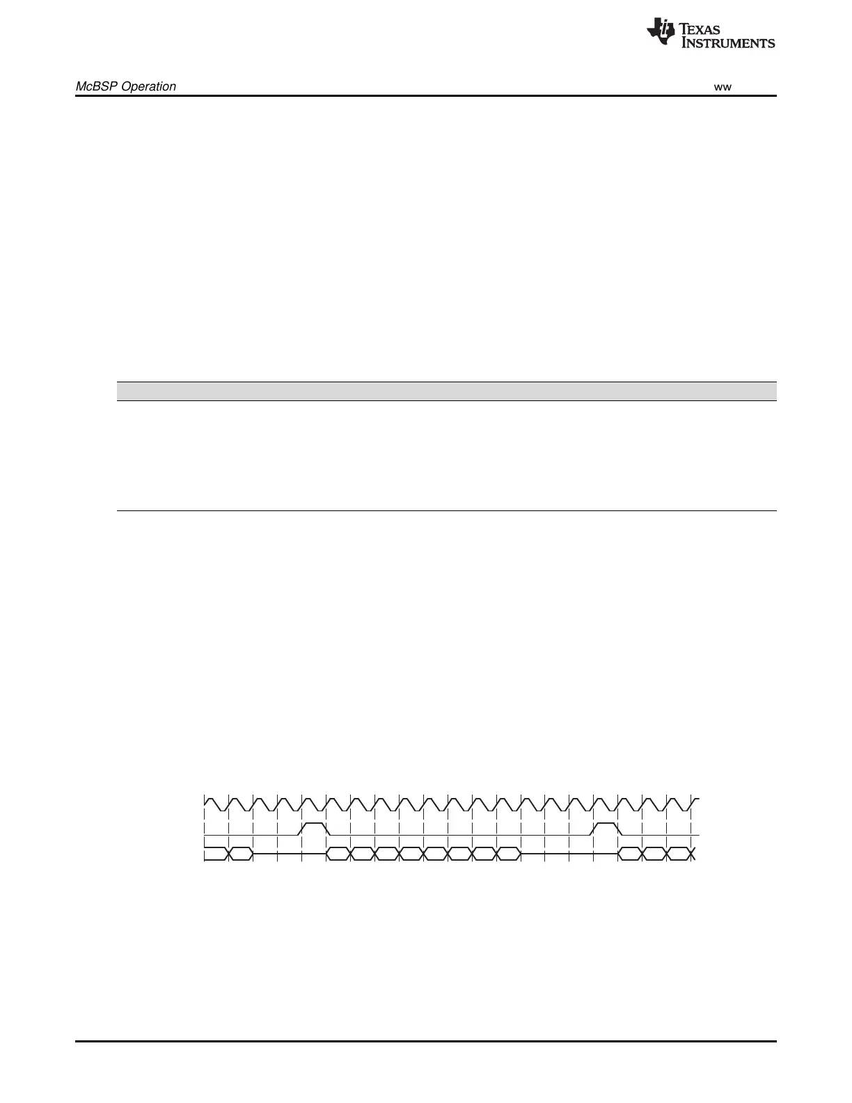
Figure 12-9 shows an example of a single-phase data frame containing one 8-bit word. Because the
transfer is configured for one data bit delay, the data on the DX and DR pins are available one clock cycle
after FS(R/X) goes active. The figure makes the following assumptions:
• (R/X)PHASE = 0: Single-phase frame
• (R/X)FRLEN1 = 0b: 1 word per frame
• (R/X)WDLEN1 = 000b: 8-bit word length
• (R/X)FRLEN2 and (R/X)WDLEN2 are ignored
• CLK(X/R)P = 0: Receive data clocked on falling edge; transmit data clocked on rising edge
• FS(R/X)P = 0: Active-high frame-synchronization signals
• (R/X)DATDLY = 01b: 1-bit data delay
Figure 12-9. Single-Phase Frame for a McBSP Data Transfer
12.3.4.3 Dual-Phase Frame Example
Figure 12-10 shows an example of a frame where the first phase consists of two words of 12 bits each,
followed by a second phase of three words of 8 bits each. The entire bit stream in the frame is contiguous.
There are no gaps either between words or between phases.
 Loading...