Clocking and System Control
www.ti.com
60
SPRUI07–March 2020
Submit Documentation Feedback
Copyright © 2020, Texas Instruments Incorporated
System Control and Interrupts
(1)
All of the registers in this table are EALLOW protected. See Section 1.5.2 for more information.
(2)
The PLL control register (PLLCR) and PLL Status Register (PLLSTS) are reset to a known state by the XRS signal or a watchdog reset
only. A reset issued by the debugger or the missing clock detect logic have no effect.
Table 1-14. PLL, Clocking, Watchdog, and Low-Power Mode Registers
Name Address Size (x16) Description
(1)
Bit Description
PLLSTS
(2)
0x7011 1 PLL Status Register Figure 1-24
HISPCP 0x701A 1 High-Speed Peripheral Clock (HSPCLK) Prescaler Register Figure 1-17
LOSPCP 0x701B 1 Low-Speed Peripheral Clock (LSPCLK) Prescaler Register Figure 1-18
PCLKCR0 0x701C 1 Peripheral Clock Control Register 0 Figure 1-14
PCLKCR1 0x701D 1 Peripheral Clock Control Register 1 Figure 1-15
LPMCR0 0x701E 1 Low Power Mode Control Register 0 Figure 1-18
PCLKCR3 0x7020 1 Peripheral Clock Control Register 3 Figure 1-16
PLLCR
(2)
0x7021 1 PLL Control Register Figure 1-23
SCSR 0x7022 1 System Control & Status Register Figure 1-27
WDCNTR 0x7023 1 Watchdog Counter Register. Figure 1-28
WDKEY 0x7025 1 Watchdog Reset Key Register Figure 1-29
WDCR 0x7029 1 Watchdog Control Register Figure 1-30
1.3.1.1 Enabling/Disabling Clocks to the Peripheral Modules
The PCLKCR0 /1/3 registers enable/disable clocks to the various peripheral modules. There is a 2-
SYSCLKOUT cycle delay from when a write to the PCLKCR0 /1/3 registers occurs to when the action is
valid. This delay must be taken into account before attempting to access the peripheral configuration
registers. Due to the peripheral/GPIO MUXing, all peripherals cannot be used at the same time. While it is
possible to turn on the clocks to all the peripherals at the same time, such a configuration is not useful. If
this is done, the current drawn will be more than required. To avoid this, only enable the clocks required
by the application.
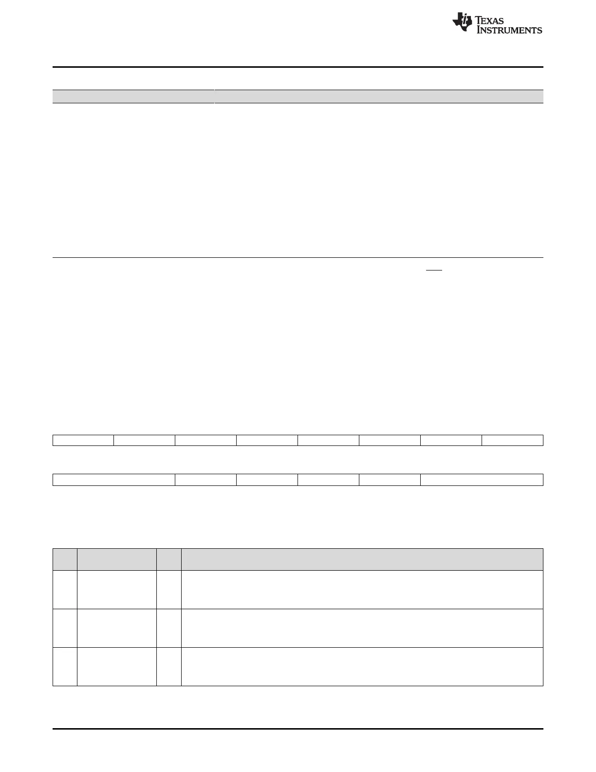
Figure 1-14. Peripheral Clock Control 0 Register (PCLKCR0)
15 14 13 12 11 10 9 8
ECANBENCLK ECANAENCLK MCBSPBENCLK MCBSPAENCLK SCIBENCLK SCIAENCLK Reserved SPIAENCLK
R/W-0 R/W-0 R/W-0 R/W-0 R/W-0 R/W-0 R-0 R/W-0
7 6 5 4 3 2 1 0
Reserved SCICENCLK I2CAENCLK ADCENCLK TBCLKSYNC Reserved
R-0 R/W-0 R/W-0 R/W-0 R/W-0 R-0
LEGEND: R/W = Read/Write; R = Read only; -n = value after reset
(1)
This register is EALLOW protected. See Section 1.5.2 for more information.
(2)
If a peripheral block is not used, the clock to that peripheral can be turned off to minimize power consumption.
(3)
On devices without a particular peripheral, the clock selection bit is reserved. On these devices, the bit should not be written to with a 1.
Table 1-15. Peripheral Clock Control 0 Register (PCLKCR0) Field Descriptions
Bit Field Valu
e
Description
(1)
15 ECANBENCLK ECAN-B Clock enable
0 The eCAN-B module is not clocked. (default)
(2)
1 The eCAN-B module is clocked (SYSCLKOUT/2).
14 ECANAENCLK ECAN-A clock enable
0 The eCAN-A module is not clocked. (default)
(2)
1 The eCAN-A module is clocked (SYSCLKOUT/2).
13 MCBSPBENCLK McBSP-B Clock Enable. This bit is reserved on devices without the McBSP-B module.
(3)
0 The McBSP-B module is not clocked. (default)
1 The McBSP-B module is clocked by the low-speed clock (LSPCLK).
 Loading...