www.ti.com
Flash and OTP Memory Blocks
47
SPRUI07–March 2020
Submit Documentation Feedback
Copyright © 2020, Texas Instruments Incorporated
System Control and Interrupts
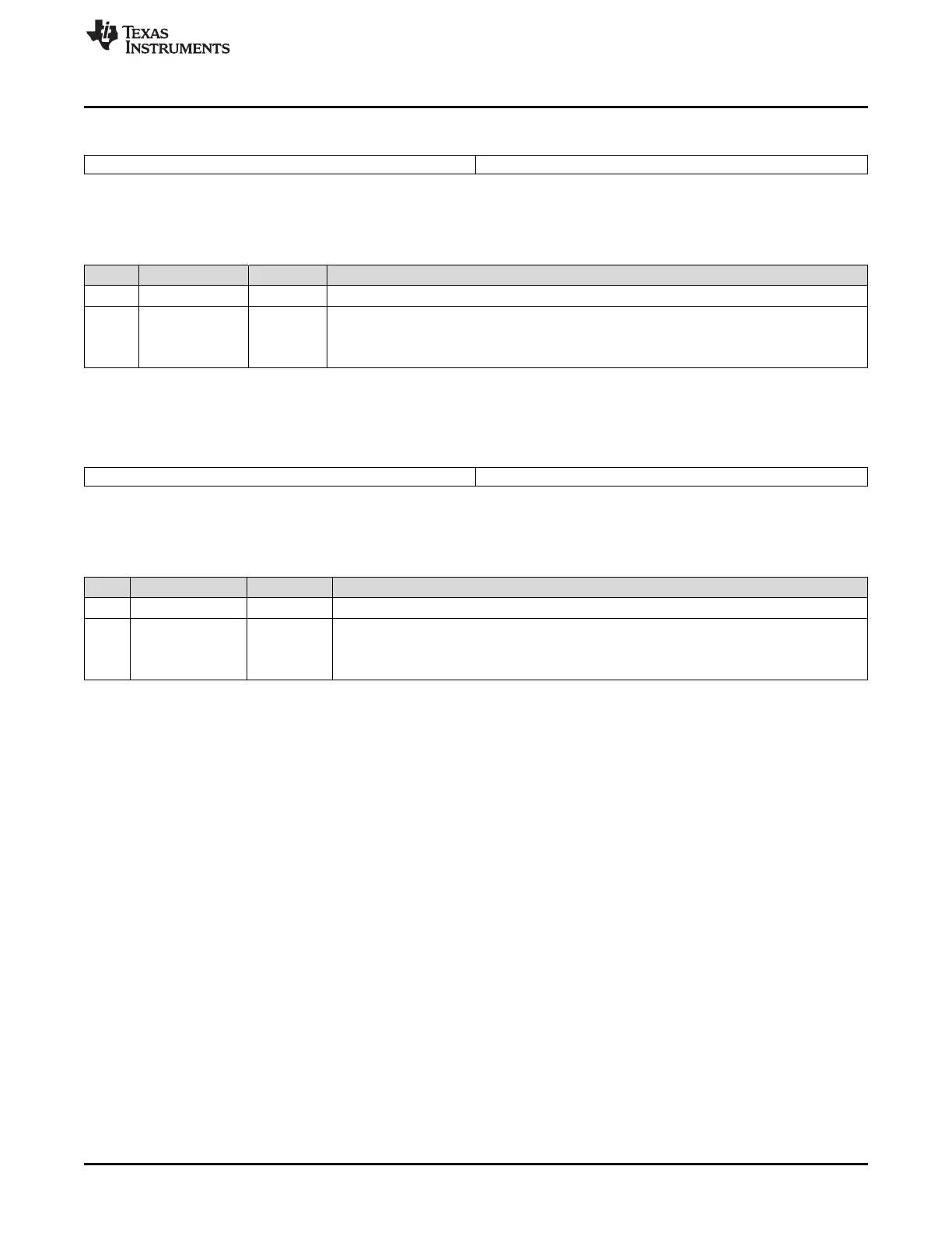
Figure 1-7. Flash Standby Wait Register (FSTDBYWAIT)
15 9 8 0
Reserved STDBYWAIT
R-0 R/W-0x1FF
LEGEND: R/W = Read/Write; R = Read only; -n = value after reset
(1)
This register is EALLOW protected. See Section 1.5.2 for more information.
(2)
This register is protected by the Code Security Module (CSM). See Section 1.2 for more information.
Table 1-5. Flash Standby Wait Register (FSTDBYWAIT) Field Descriptions
Bit Field Value Description
(1) (2)
15-9 Reserved 0 Reserved
8-0 STDBYWAIT This register should be left in its default state.
Bank and Pump Sleep To Standby Wait Count.
111111111 511 SYSCLKOUT cycles (default)
Figure 1-8. Flash Standby to Active Wait Counter Register (FACTIVEWAIT)
7 9 8 0
Reserved ACTIVEWAIT
R-0 R/W-0x1FF
LEGEND: R/W = Read/Write; R = Read only; -n = value after reset
(1)
This register is EALLOW protected. See Section 1.5.2 for more information.
(2)
This register is protected by the Code Security Module (CSM). See Section 1.2 for more information.
Table 1-6. Flash Standby to Active Wait Counter Register (FACTIVEWAIT) Field Descriptions
Bits Field Value Description
(1) (2)
15-9 Reserved 0 Reserved
8-0 ACTIVEWAIT This register should be left in its default state.
Bank and Pump Standby To Active Wait Count:
111111111 511 SYSCLKOUT cycles (default)
 Loading...