RX FIFO 15
RX FIFO 0
RX BUF
RXSHF
TX FIFO 15
TX FIFO 0
TX
RX
16x8 bit FIFO
RXFFOVF flag
RXFFIL
RXERR flag
RXRDY/BRKDT
TXFFIL
1
0
RXINT
RXFFIENA
RXERRINTENA
RX/BKINTENA
TXFFIENA
TX BUF
TXSHF
SCIFFENA
TXRDY flag
TXINTENA
SCIFFENA
0
1
TXINT
Auto-baud
detect logic
ABD bit
CDC bit
www.ti.com
SCI Enhanced Features
593
SPRUI07–March 2020
Submit Documentation Feedback
Copyright © 2020, Texas Instruments Incorporated
Serial Communications Interface (SCI)
a minimum delay of 0 baud clock cycles and a maximum of 256-baud clock cycles. With zero delay,
the SCI module can transmit data in continuous mode with the FIFO words shifting out back to back.
With the 256 clock delay the SCI module can transmit data in a maximum delayed mode with the FIFO
words shifting out with a delay of 256 baud clocks between each words. The programmable delay
facilitates communication with slow SCI/UARTs with little CPU intervention.
8. FIFO status bits. Both the transmit and receive FIFOs have status bits TXFFST or RXFFST (bits 12−8)
that define the number of words available in the FIFOs at any time. The transmit FIFO reset bit
TXFIFO and receive reset bit RXFIFO reset the FIFO pointers to zero when these bits are cleared to 0.
The FIFOs resumes operation from start once these bits are set to one.
9. Programmable interrupt levels. Both transmit and receive FIFO can generate CPU interrupts. The
interrupt trigger is generated whenever the transmit FIFO status bits TXFFST (bits 12−8) match (less
than or equal to) the interrupt trigger level bits TXFFIL (bits 4−0 ). This provides a programmable
interrupt trigger for transmit and receive sections of the SCI. Default value for these trigger level bits
will be 0x11111 for receive FIFO and 0x00000 for transmit FIFO, respectively.
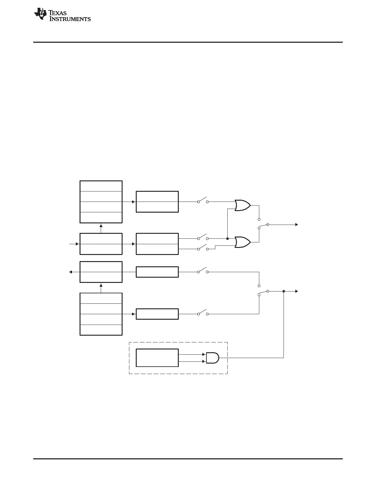
Figure 10-10 and Table 10-4 explain the operation/configuration of SCI interrupts in nonFIFO/FFO mode.
Figure 10-10. SCI FIFO Interrupt Flags and Enable Logic
 Loading...