www.ti.com
McBSP Registers
747
SPRUI07–March 2020
Submit Documentation Feedback
Copyright © 2020, Texas Instruments Incorporated
Multichannel Buffered Serial Port (McBSP)
12.15.2 Data Receive Registers (DRR[1,2])
The CPU or the DMA controller reads received data from one or both of the data receive registers (see
Figure 12-67). If the serial word length is 16 bits or smaller, only DRR1 is used. If the serial length is larger
than 16 bits, both DRR1 and DRR2 are used and DRR2 holds the most significant bits. Each frame of
receive data in the McBSP can have one phase or two phases, each with its own serial word length.
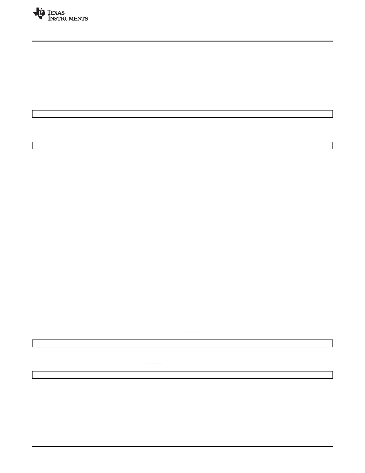
Figure 12-67. Data Receive Registers (DRR2 and DRR1)
DDR2
15 0
High part of receive data (for 20-, 24- or 32-bit data)
R/W-0
DDR1
15 0
Receive data (for 8-, 12-, or 16-bit data) or low part of receive data (for 20-, 24- or 32-bit data)
R/W-0
LEGEND: R/W = Read/Write; R = Read only; -n = value after reset
12.15.2.1 Data Travel From Data Receive Pins to the Registers
If the serial word length is 16 bits or smaller, receive data on the MDRx pin is shifted into receive shift
register 1 (RSR1) and then copied into receive buffer register 1 (RBR1). The content of RBR1 is then
copied to DRR1, which can be read by the CPU or by the DMA controller. The RSRs and RBRs are not
accessible to the user.
If the serial word length is larger than 16 bits, receive data on the MDRx pin is shifted into both of the
receive shift registers (RSR2, RSR1) and then copied into both of the receive buffer registers (RBR2,
RBR1). The content of the RBRs is then copied into both of the DRRs, which can be read by the CPU or
by the DMA controller.
If companding is used during the copy from RBR1 to DRR1 (RCOMPAND = 10b or 11b), the 8-bit
compressed data in RBR1 is expanded to a left-justified 16-bit value in DRR1. If companding is disabled,
the data copied from RBR[1,2] to DRR[1,2] is justified and bit filled according to the RJUST bits.
12.15.3 Data Transmit Registers (DXR[1,2])
For transmission, the CPU or the DMA controller writes data to one or both of the data transmit registers
(see Figure 12-68). If the serial word length is 16 bits or smaller, only DXR1 is used. If the word length is
larger than 16 bits, both DXR1 and DXR2 are used and DXR2 holds the most significant bits. Each frame
of transmit data in the McBSP can have one phase or two phases, each with its own serial word length.
Figure 12-68. Data Transmit Registers (DXR2 and DXR1)
DXR2
15 0
High part of transmit data (for 20-, 24- or 32-bit data)
R/W-0
DXR1
15 0
Transmit data (for 8-, 12-, or 16-bit data) or low part of receive data (for 20-, 24- or 32-bit data)
R/W-0
LEGEND: R/W = Read/Write; R = Read only; -n = value after reset
 Loading...