GPADAT
(latch)
GPACLEAR
GPATOGGLE
GPAQSEL 1/2
Qual
GPAMUX 1/2
SYSCLKOUT
High-
Impedance
Output
Control
GPIO28,
GPIO29,
GPIO30,
GPIO31
Pins
PU
XRS
0 = Input , 1 = Output
Sync
LowPower
ModesBlock
GPIOx.async
GPADIR
(latch)
01
11
01
01
0x
1x
01
GPACTRL
2
2
10
Perpheral1input
N/C
(defaultonreset)
(defaultonreset)
GPIOx_OUT
GPIOx_DIR
GPAPUD
0 = enablePU
1 = disablePU
(disabledafterreset)
async
(asyncdisable
whenlow)
0x
1x
11
10
XINTFOutputSignals
XZCS6,XA19,XA18,XA17
1
N/C
N/C
Perpheral1output
Perpheral1ouputenable
GPASET
(defaultonreset)
3samples
6samples
LPMCR0
GPIOLPMSEL
00
00
00
00
XRS
DefaultatReset
External
interrupt
MUX
GPIOXINT2SEL
GPIOXNMISEL
GPIOXINT1SEL
PIE
GPADAT (read)
General-Purpose Input/Output (GPIO)
www.ti.com
88
SPRUI07–March 2020
Submit Documentation Feedback
Copyright © 2020, Texas Instruments Incorporated
System Control and Interrupts
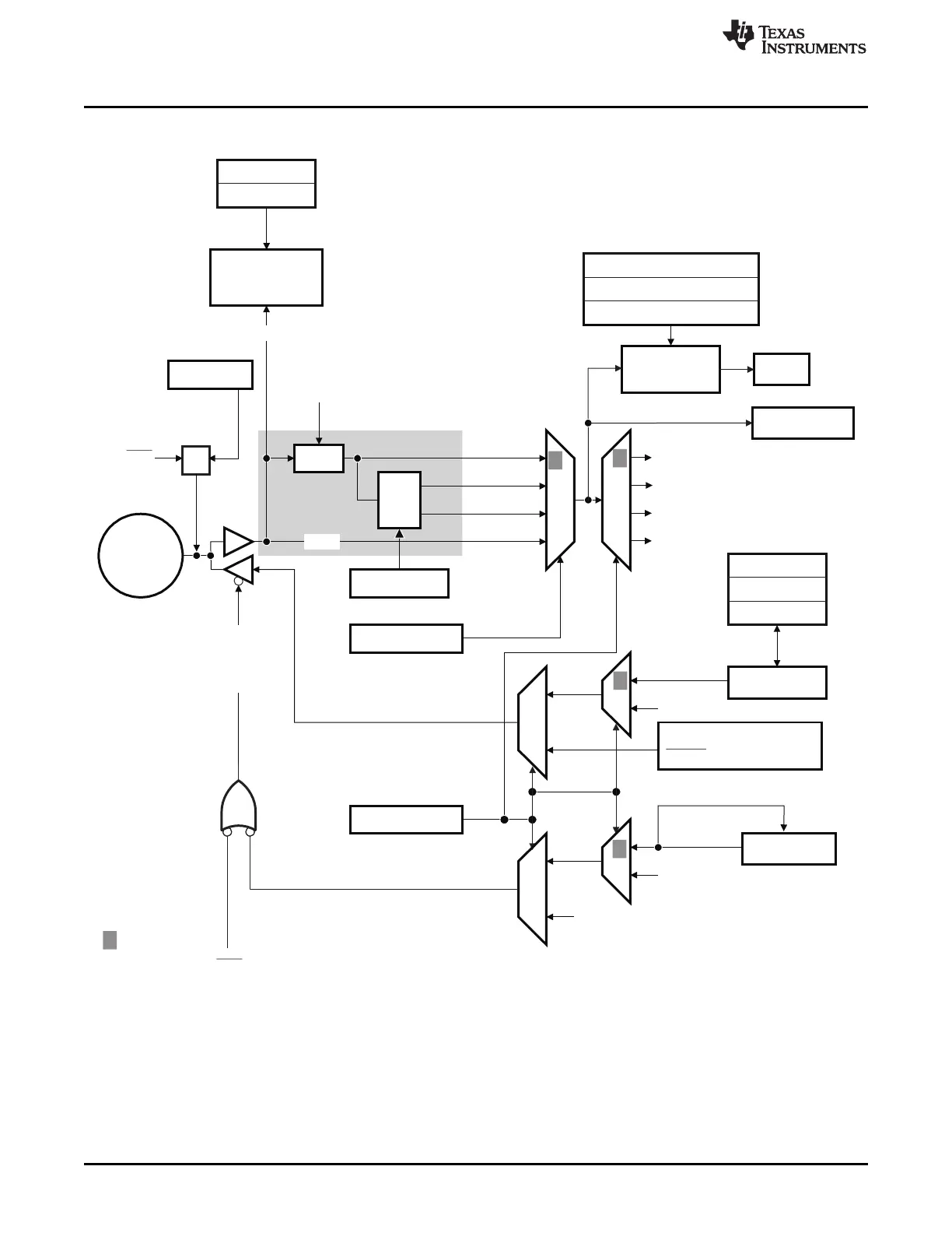
Figure 1-41. GPIO28 to GPIO31 Multiplexing Diagram (Peripheral 2 and Peripheral 3 Outputs Merged)
A The shaded area is disabled in the above GPIOs when the GPIOINENCLK bit is cleared to 0 in the PCLKCR3 register
and the respective pin is configured as an output. This is to reduce power consumption when a pin is configured as
an output. Clearing the GPIOINCLK bit will reset the sync and qualification logic so no residual value is left.
B The input qualification circuit is not reset when modes are changed (such as changing from output to input mode).
Any state will get flushed by the circuit eventually.
 Loading...