www.ti.com
SPI Registers
579
SPRUI07–March 2020
Submit Documentation Feedback
Copyright © 2020, Texas Instruments Incorporated
Serial Peripheral Interface (SPI)
9.5.2.11 SPIFFCT Register (Offset = Ch) [reset = 0h]
SPIFFCT is shown in Figure 9-18 and described in Table 9-17.
Return to the Summary Table.
SPIFFCT controls the FIFO transmit delay bits.
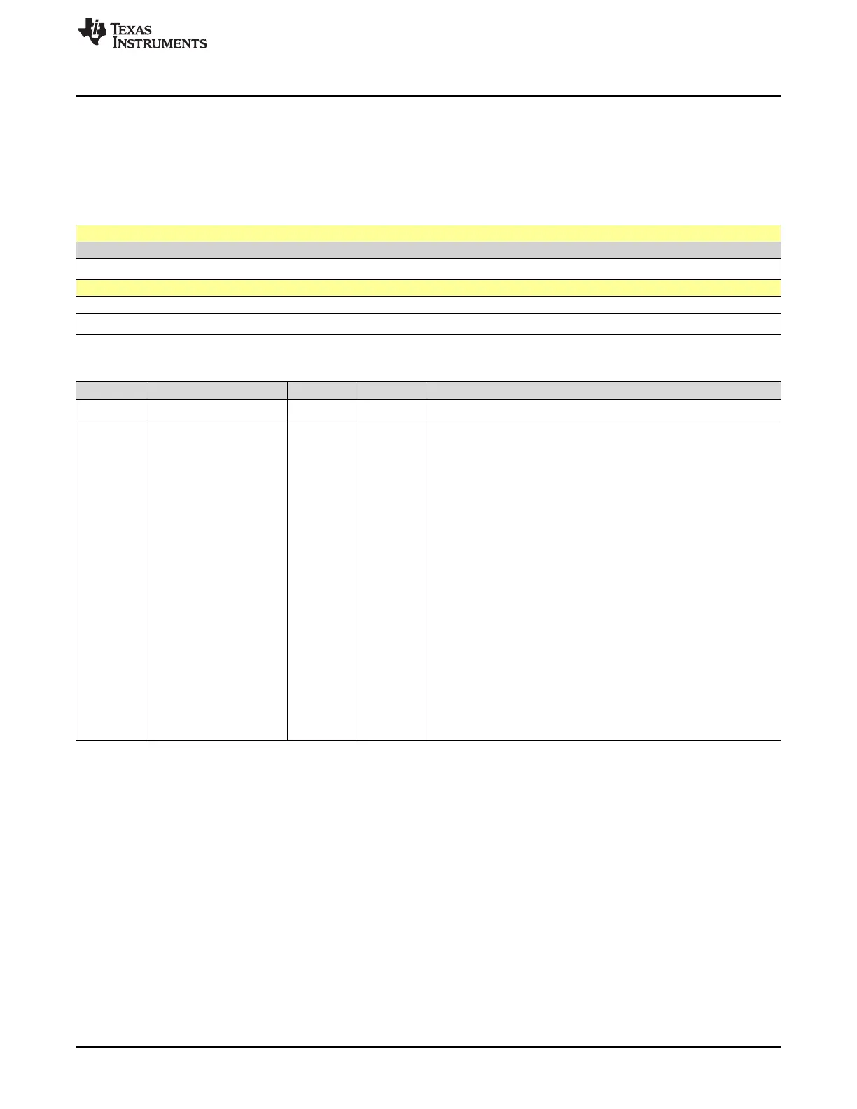
Figure 9-18. SPIFFCT Register
15 14 13 12 11 10 9 8
RESERVED
R-0h
7 6 5 4 3 2 1 0
TXDLY
R/W-0h
Table 9-17. SPIFFCT Register Field Descriptions
Bit Field Type Reset Description
15-8 RESERVED R 0h
Reserved
7-0 TXDLY R/W 0h
FIFO Transmit Delay Bits
These bits define the delay between every transfer from FIFO
transmit buffer to transmit shift register. The delay is defined in
number SPI serial clock cycles. The 8-bit register could define a
minimum delay of 0 serial clock cycles and a maximum of 255 serial
clock cycles. In FIFO mode, the buffer (TXBUF) between the shift
register and the FIFO should be filled only after the shift register has
completed shifting of the last bit. This is required to pass on the
delay between transfers to the data stream. In the FIFO mode
TXBUF should not be treated as one additional level of buffer.
Reset type: SYSRSn
0h (R/W) = The next word in the TX FIFO buffer is transferred to
SPITXBUF immediately upon completion of transmission of the
previous word.
1h (R/W) = The next word in the TX FIFO buffer is transferred to
SPITXBUF1 serial clock cycle after completion of transmission of
the previous word.
2h (R/W) = The next word in the TX FIFO buffer is transferred to
SPITXBUF 2 serial clock cycles after completion of transmission of
the previous word.
FFh (R/W) = The next word in the TX FIFO buffer is transferred to
SPITXBUF 255 serial clock cycles after completion of transmission
of the previous word.
 Loading...