X1
XCLKIN
(3.3-Vclockinput
fromexternal
oscillator)
On-chip
oscillator
X2
PLLSTS[OSCOFF]
OSCCLK
PLL
VCOCLK
4-bitMultiplierPLLCR[DIV]
OSCCLKor
VCOCLK
CLKIN
OSCCLK
0
PLLSTS[PLLOFF]
n
n ≠ 0
PLLSTS[DIVSEL]
/1
/2
/4
External
Crystalor
Resonator
To
CPU
Clocking and System Control
www.ti.com
66
SPRUI07–March 2020
Submit Documentation Feedback
Copyright © 2020, Texas Instruments Incorporated
System Control and Interrupts
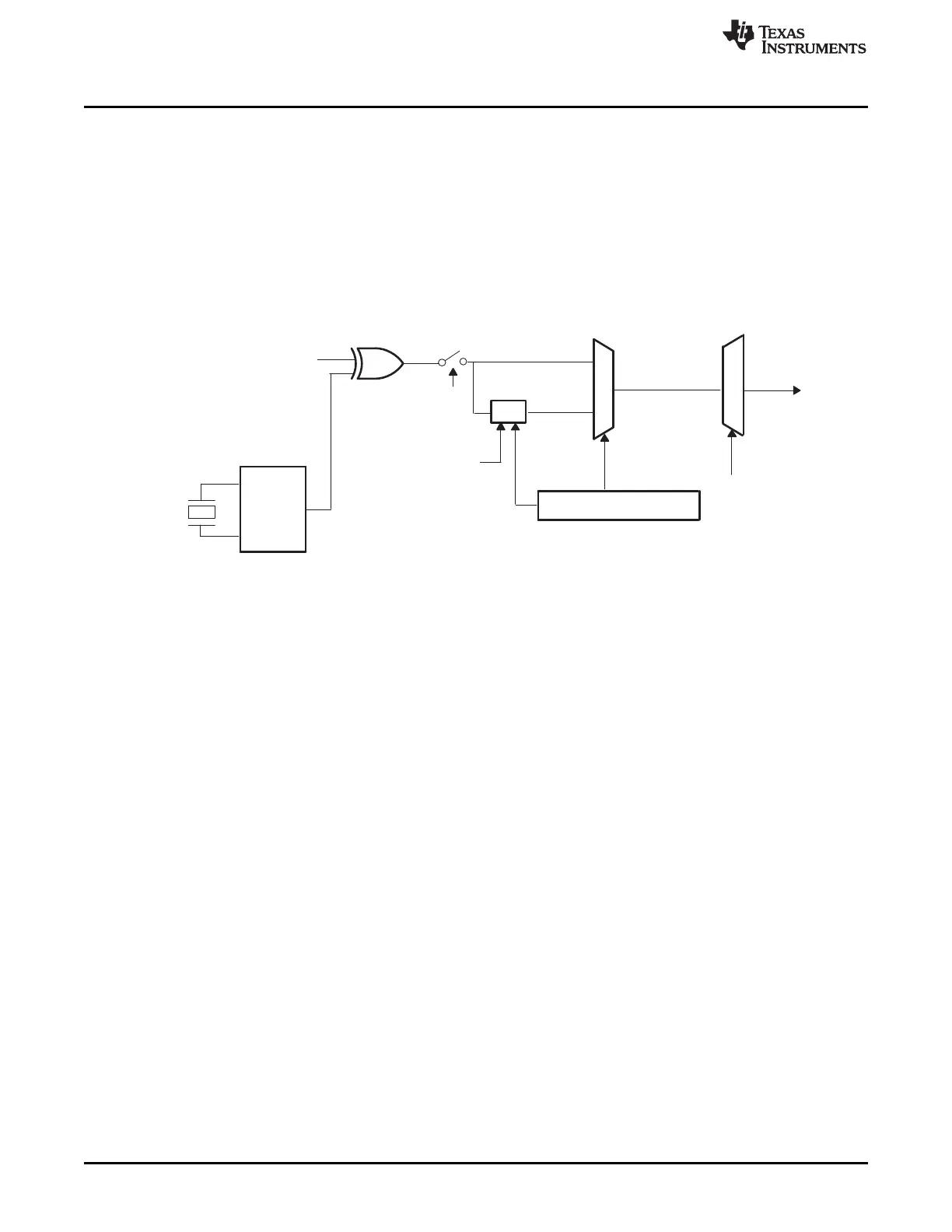
1.3.2 OSC and PLL Block
The on-chip oscillator and phase-locked loop (PLL) block provides the clocking signals for the device, as
well as control for low-power mode (LPM) entry.
1.3.2.1 PLL-Based Clock Module
The 2833x, 2823x devices have an on-chip, PLL-based clock module. The PLL has a 4-bit ratio control to
select different CPU clock rates. Figure 1-19 shows the OSC and PLL block.
Figure 1-19. OSC and PLL Block
The PLL-based clock module provides two modes of operation:
• Crystal/Resonator Operation:
The on-chip oscillator enables the use of an external crystal/resonator to be attached to the device to
provide the time base to the device. The crystal/resonator is connected to the X1/X2 pins and XCLKIN
is tied low.
• External clock source operation:
If the on-chip oscillator is not used, this mode allows the internal oscillator to be bypassed. The device
clocks are generated from an external clock source input on either the X1 or the XCLKIN pin.
Option 1: External clock on the XCLKIN pin:
When using XCLKIN as the external clock source, you must tie X1 low and leave X2 disconnected. In
this case, an external oscillator clock is connected to the XCLKIN pin, which allows for a 3.3-V clock
source to be used.
Option 2: External clock on the X1 pin:
When using X1 as the clock source, you must tie XCLKIN low and leave X2 disconnected. In this case,
an external oscillator clock is connected to the X1 pin, which allows for a 1.8-V clock source to be
used.
The OSC circuit enables attachment of a crystal using the X1 and X2 pins. If a crystal is not used, then an
external oscillator can be directly connected to the XCLKIN pin, the X2 pin is left unconnected, and the X1
pin is tied low. See the TMS320F28335, TMS320F28334, TMS28332, TMS320F28235, TMS320F28234,
TMS28232 Digital Signal Controllers (DSCs) Data Manual (literature number SPRS439). The input clock
and PLLCR[DIV] bits should be chosen in such a way that the output frequency of the PLL (VCOCLK)
does not exceed 300 MHz .
 Loading...