www.ti.com
General-Purpose Input/Output (GPIO)
125
SPRUI07–March 2020
Submit Documentation Feedback
Copyright © 2020, Texas Instruments Incorporated
System Control and Interrupts
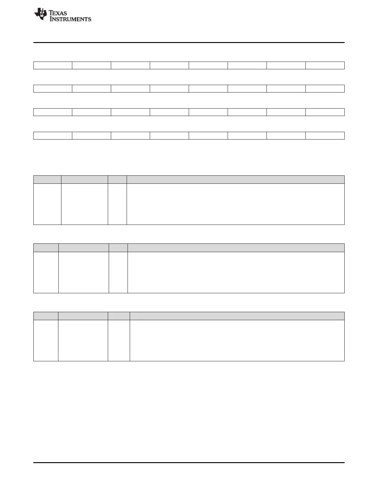
Figure 1-69. GPIO Port B Set, Clear and Toggle (GPBSET, GPBCLEAR, GPBTOGGLE) Registers
31 30 29 28 27 26 25 24
GPIO63 GPIO62 GPIO61 GPIO60 GPIO59 GPIO58 GPIO57 GPIO56
R/W-x R/W-x R/W-x R/W-x R/W-x R/W-x R/W-x R/W-x
23 22 21 20 19 18 17 16
GPIO55 GPIO54 GPIO53 GPIO52 GPIO51 GPIO50 GPIO49 GPIO48
R/W-x R/W-x R/W-x R/W-x R/W-x R/W-x R/W-x R/W-x
15 14 13 12 11 10 9 8
GPIO47 GPIO46 GPIO45 GPIO44 GPIO43 GPIO42 GPIO41 GPIO40
R/W-x R/W-x R/W-x R/W-x R/W-x R/W-x R/W-x R/W-x
7 6 5 4 3 2 1 0
GPIO39 GPIO38 GPIO37 GPIO36 GPIO35 GPIO34 GPIO33 GPIO32
R/W-x R/W-x R/W-x R/W-x R/W-x R/W-x R/W-x R/W-x
LEGEND: R/W = Read/Write; R = Read only; -n = value after reset
Table 1-74. GPIO Port B Set (GPBSET) Register Field Descriptions
Bits Field Value Description
31-0 GPIO63-GPIO32 Each GPIO port B pin (GPIO32-GPIO63) corresponds to one bit in this register as shown in
Figure 1-69.
0 Writes of 0 are ignored. This register always reads back a 0.
1 Writing a 1 forces the respective output data latch to high. If the pin is configured as a GPIO
output then it will be driven high. If the pin is not configured as a GPIO output then the latch is
set but the pin is not driven.
Table 1-75. GPIO Port B Clear (GPBCLEAR) Register Field Descriptions
Bits Field Value Description
31-0 GPIO63-GPIO32 Each GPIO port B pin (GPIO32-GPIO63) corresponds to one bit in this register as shown in
Figure 1-69.
0 Writes of 0 are ignored. This register always reads back a 0.
1 Writing a 1 forces the respective output data latch to low. If the pin is configured as a GPIO
output then it will be driven low. If the pin is not configured as a GPIO output then the latch is
cleared but the pin is not driven.
Table 1-76. GPIO Port B Toggle (GPBTOGGLE) Register Field Descriptions
Bits Field Value Description
31-0 GPIO63-GPIO32 Each GPIO port B pin (GPIO32-GPIO63) corresponds to one bit in this register as shown in
Figure 1-69.
0 Writes of 0 are ignored. This register always reads back a 0.
1 Writing a 1 forces the respective output data latch to toggle from its current state. If the pin is
configured as a GPIO output then it will be driven in the opposite direction of its current state. If
the pin is not configured as a GPIO output then the latch is cleared but the pin is not driven.
 Loading...