D(R/X)
FS(R/X)
CLK(R/X)
B0B1B2B3B4B5B6B7A0A1
(1)
(2) (DLB)
From CPU or DMA controller
DXR1
To CPU or DMA controller
DRR1
DX
XSR1
Compress
Expand
DR
RBR1RSR1
www.ti.com
McBSP Operation
663
SPRUI07–March 2020
Submit Documentation Feedback
Copyright © 2020, Texas Instruments Incorporated
Multichannel Buffered Serial Port (McBSP)
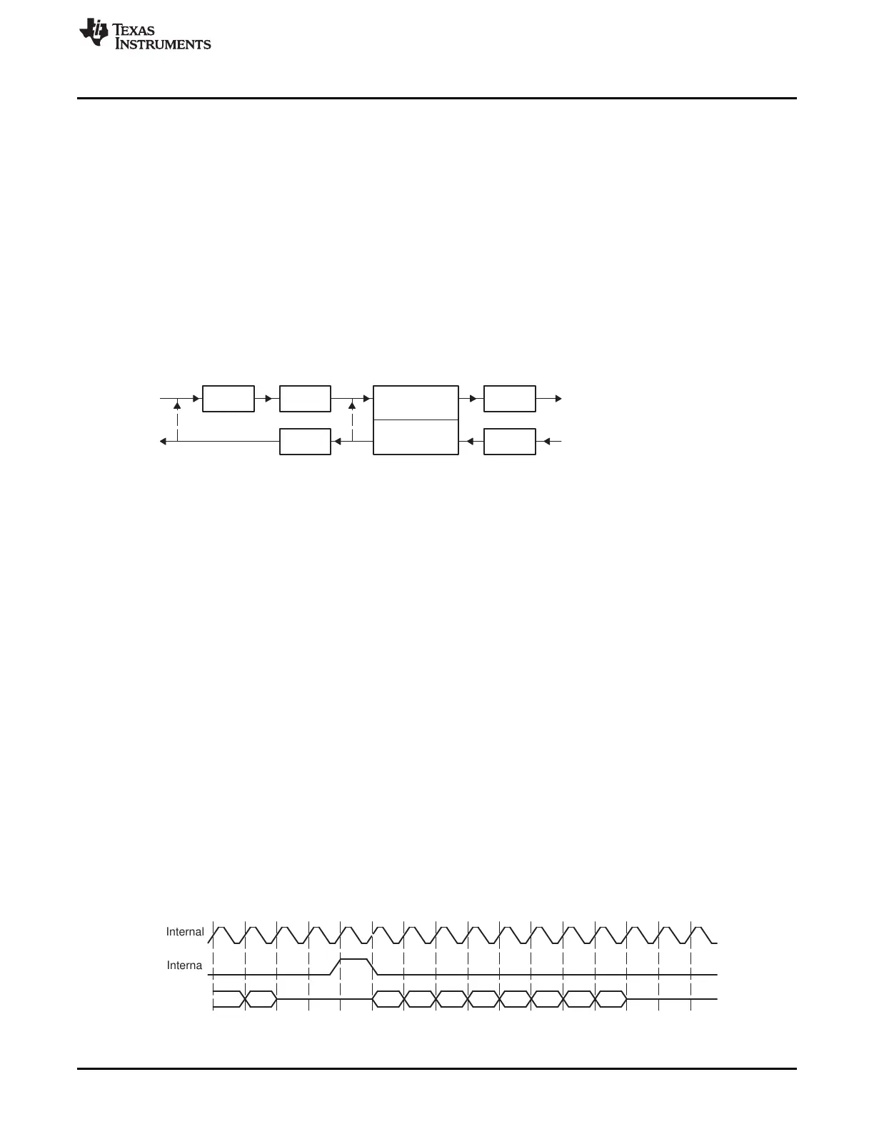
Figure 12-6 shows two methods by which the McBSP can compand internal data. Data paths for these
two methods are used to indicate:
• When both the transmit and receive sections of the serial port are reset, DRR1 and DXR1 are
connected internally through the companding logic. Values from DXR1 are compressed, as selected by
XCOMPAND, and then expanded, as selected by RCOMPAND. RRDY and XRDY bits are not set.
However, data is available in DRR1 within four CPU clocks after being written to DXR1.
The advantage of this method is its speed. The disadvantage is that there is no synchronization
available to the CPU and DMA to control the flow. DRR1 and DXR1 are internally connected if the
(X/R)COMPAND bits are set to 10b or 11b (compand using μ-law or A-law).
• The McBSP is enabled in digital loopback mode with companding appropriately enabled by
RCOMPAND and XCOMPAND. Receive and transmit interrupts (RINT when RINTM = 0 and XINT
when XINTM = 0) or synchronization events (REVT and XEVT) allow synchronization of the CPU or
DMA to these conversions, respectively. Here, the time for this companding depends on the serial bit
rate selected.
Figure 12-6. Two Methods by Which the McBSP Can Compand Internal Data
12.3.2.3 Reversing Bit Order: Option to Transfer LSB First
Generally, the McBSP transmits or receives all data with the most significant bit (MSB) first. However,
certain 8-bit data protocols (that do not use companded data) require the least significant bit (LSB) to be
transferred first. If you set XCOMPAND = 01b in XCR2, the bit ordering of 8-bit words is reversed (LSB
first) before being sent from the serial port. If you set RCOMPAND = 01b in RCR2, the bit ordering of 8-bit
words is reversed during reception. Similar to companding, this feature is enabled only if the appropriate
word length bits are set to 0, indicating that 8-bit words are to be transferred serially. If either phase of the
frame does not have an 8-bit word length, the McBSP assumes the word length is eight bits, and LSB-first
ordering is done.
12.3.3 Clocking and Framing Data
This section explains basic concepts and terminology important for understanding how McBSP data
transfers are timed and delimited.
12.3.3.1 Clocking
Data is shifted one bit at a time from the DR pin to the RSR(s) or from the XSR(s) to the DX pin. The time
for each bit transfer is controlled by the rising or falling edge of a clock signal.
The receive clock signal (CLKR) controls bit transfers from the DR pin to the RSR(s). The transmit clock
signal (CLKX) controls bit transfers from the XSR(s) to the DX pin. CLKR or CLKX can be derived from a
pin at the boundary of the McBSP or derived from inside the McBSP. The polarities of CLKR and CLKX
are programmable.
Figure 12-7 shows how the clock signal controls the timing of each bit transfer on the pin.
Figure 12-7. Example - Clock Signal Control of Bit Transfer Timing
 Loading...