SPI master (master/slave = 1) SPI slave (master/slave = 0)
SPIRXBUF.15−0
Serial input buffer
SPIRXBUF
Shift register
(SPIDAT)
SPITXBUF.15−0
Serial transmit buffer
SPITXBUF
Processor 1
SPIDAT.15−0
SPICLK
SPISOMI
SPISTE
SPISIMO
SPICLK
SPISOMI
SPISTE
SPISIMO
Slave in/
master out
SPI
strobe
Slave out/
master in
Serial
clock
SPIRXBUF.15−0
Serial input buffer
SPIRXBUF
Shift register
(SPIDAT)
SPITXBUF.15−0
Serial transmit buffer
SPITXBUF
SPIDAT.15−0
Processor 2
LSBMSB LSBMSB
www.ti.com
SPI Operation
553
SPRUI07–March 2020
Submit Documentation Feedback
Copyright © 2020, Texas Instruments Incorporated
Serial Peripheral Interface (SPI)
9.3 SPI Operation
This section describes the various modes of operation of the SPI. Included are explanations of the
operational modes, interrupts, data format, clock sources, and initialization. Typical timing diagrams for
data transfers are given.
9.3.1 Introduction to Operation
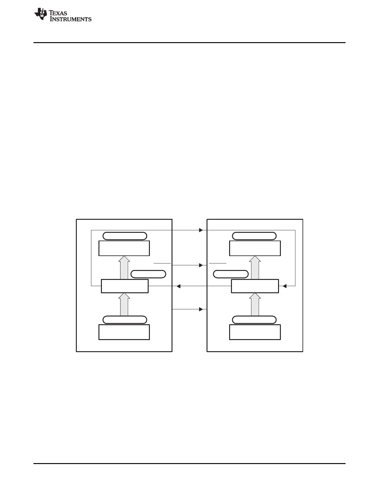
Figure 9-3 shows typical connections of the SPI for communications between two controllers: a master
and a slave.
The master transfers data by sending the SPICLK signal. For both the slave and the master, data is
shifted out of the shift registers on one edge of the SPICLK and latched into the shift register on the
opposite SPICLK clock edge. If the CLK_PHASE bit is high, data is transmitted and received a half-cycle
before the SPICLK transition. As a result, both controllers send and receive data simultaneously. The
application software determines whether the data is meaningful or dummy data. There are three possible
methods for data transmission:
• Master sends data; slave sends dummy data.
• Master sends data; slave sends data.
• Master sends dummy data; slave sends data.
The master can initiate data transfer at any time because it controls the SPICLK signal. The software,
however, determines how the master detects when the slave is ready to broadcast data.
Figure 9-3. SPI Master/Slave Connection
The SPI can operate in master or slave mode. The MASTER_SLAVE bit selects the operating mode and
the source of the SPICLK signal.
Figure 9-4 is a block diagram of the SPI module showing all of the basic control blocks available on the
SPI module.
 Loading...