Emulation and Reset Considerations
www.ti.com
736
SPRUI07–March 2020
Submit Documentation Feedback
Copyright © 2020, Texas Instruments Incorporated
Multichannel Buffered Serial Port (McBSP)
12.9.20.1 Frame Synchronization Pulses, Clock Signals, and Their Polarities
Transmit frame-synchronization pulses can be either generated internally by the sample rate generator
(see Section 12.4.2) or driven by an external source. The source of frame synchronization is selected by
programming the mode bit, FSXM, in PCR. FSX is also affected by the FSGM bit in SRGR2. For
information about the effects of FSXM and FSGM, see Section 12.9.16). Similarly, transmit clocks can be
selected to be inputs or outputs by programming the mode bit, CLKXM, in the PCR (see Section 12.9.19).
When FSR and FSX are inputs (FSXM = FSRM= 0, external frame-synchronization pulses), the McBSP
detects them on the internal falling edge of clock, internal MCLKR, and internal CLKX, respectively. The
receive data arriving at the DR pin is also sampled on the falling edge of internal MCLKR. These internal
clock signals are either derived from external source via CLK(R/X) pins or driven by the sample rate
generator clock (CLKG) internal to the McBSP.
When FSR and FSX are outputs, implying that they are driven by the sample rate generator, they are
generated (transition to their active state) on the rising edge of internal clock, CLK(R/X). Similarly, data on
the DX pin is output on the rising edge of internal CLKX.
FSRP, FSXP, CLKRP, and CLKXP in the pin control register (PCR) configure the polarities of the FSR,
FSX, MCLKR, and CLKX signals, respectively. All frame-synchronization signals (internal FSR, internal
FSX) that are internal to the serial port are active high. If the serial port is configured for external frame
synchronization (FSR/FSX are inputs to McBSP), and FSRP = FSXP = 1, the external active-low frame-
synchronization signals are inverted before being sent to the receiver (internal FSR) and transmitter
(internal FSX). Similarly, if internal synchronization (FSR/FSX are output pins and GSYNC = 0) is
selected, the internal active-high frame-synchronization signals are inverted, if the polarity bit FS(R/X)P =
1, before being sent to the FS(R/X) pin.
On the transmit side, the transmit clock polarity bit, CLKXP, sets the edge used to shift and clock out
transmit data. Data is always transmitted on the rising edge of internal CLKX. If CLKXP = 1 and external
clocking is selected (CLKXM = 0 and CLKX is an input), the external falling-edge triggered input clock on
CLKX is inverted to a rising-edge triggered clock before being sent to the transmitter. If CLKXP = 1 and
internal clocking is selected (CLKXM = 1 and CLKX is an output pin), the internal (rising-edge triggered)
clock, internal CLKX, is inverted before being sent out on the MCLKX pin.
Similarly, the receiver can reliably sample data that is clocked with a rising edge clock (by the transmitter).
The receive clock polarity bit, CLKRP, sets the edge used to sample received data. The receive data is
always sampled on the falling edge of internal MCLKR. Therefore, if CLKRP = 1 and external clocking is
selected (CLKRM = 0 and CLKR is an input pin), the external rising-edge triggered input clock on CLKR is
inverted to a falling-edge triggered clock before being sent to the receiver. If CLKRP = 1 and internal
clocking is selected (CLKRM = 1), the internal falling-edge triggered clock is inverted to a rising-edge
triggered clock before being sent out on the MCLKR pin.
CLKRP = CLKXP in a system where the same clock (internal or external) is used to clock the receiver and
transmitter. The receiver uses the opposite edge as the transmitter to ensure valid setup and hold of data
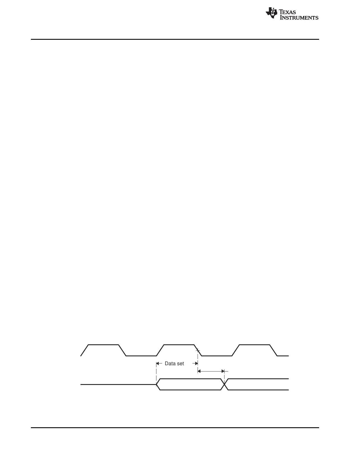
around this edge (see Figure 12-58).
Figure 12-60 shows how data clocked by an external serial device using a rising edge can be sampled by
the McBSP receiver on the falling edge of the same clock.
Figure 12-60. Data Clocked Externally Using a Rising Edge and Sampled by the McBSP Receiver on a
Falling Edge
12.10 Emulation and Reset Considerations
This section covers the following topics:
 Loading...