A C D E F G H I J
7 6 5 4 3 7 6 345
7 6 5 4 3 7 6 345
Master SPI
Int flag
Slave SPI
Int flag
SPISOMI
from slave
CLOCK POLARITY = 0
CLOCK PHASE = 0
CLOCK POLARITY = 1
CLOCK PHASE = 0
SPISIMO
from master
CLOCK POLARITY = 1
CLOCK PHASE = 1
CLOCK POLARITY = 0
CLOCK PHASE = 1
B
SPISTE
K
SPICLK signal options:
www.ti.com
Programming Procedure
561
SPRUI07–March 2020
Submit Documentation Feedback
Copyright © 2020, Texas Instruments Incorporated
Serial Peripheral Interface (SPI)
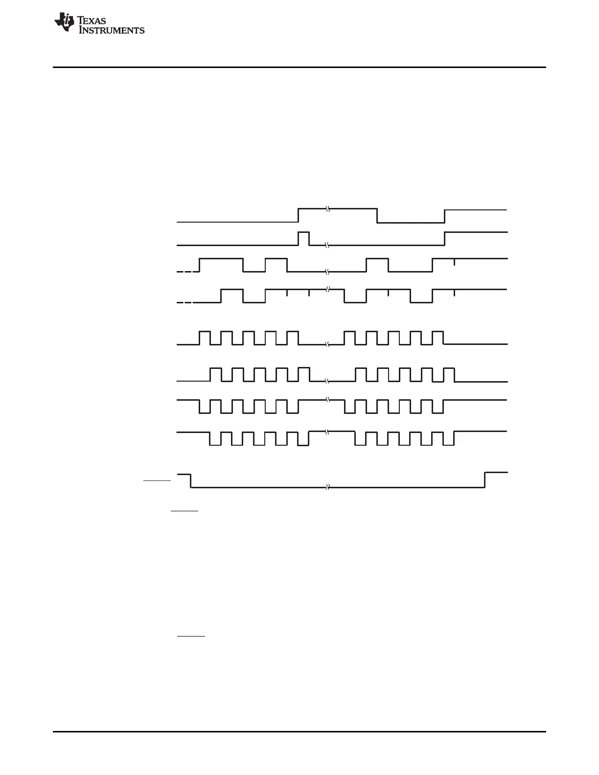
9.4.3 Data Transfer Example
The timing diagram shown in Figure 9-7 illustrates an SPI data transfer between two devices using a
character length of five bits with the SPICLK being symmetrical.
The timing diagram with SPICLK asymmetrical (Figure 9-6) shares similar characterizations with Figure 9-
7 except that the data transfer is one LSPCLK cycle longer per bit during the low pulse (CLKPOLARITY =
0) or during the high pulse (CLKPOLARITY = 1) of the SPICLK.
Figure 9-7 is applicable for 8-bit SPI only and is not for C28x devices that are capable of working with 16-
bit data. The figure is shown for illustrative purposes only.
Figure 9-7. Five Bits per Character
A Slave writes 0D0h to SPIDAT and waits for the master to shift out the data.
B Master sets the slave SPISTE signal low (active).
C Master writes 058h to SPIDAT, which starts the transmission procedure.
D First byte is finished and sets the interrupt flags.
E Slave reads 0Bh from its SPIRXBUF (right-justified).
F Slave writes 04Ch to SPIDAT and waits for the master to shift out the data.
G Master writes 06Ch to SPIDAT, which starts the transmission procedure.
H Master reads 01Ah from the SPIRXBUF (right−justified).
I Second byte is finished and sets the interrupt flags.
J Master reads 89h and the slave reads 8Dh from their respective SPIRXBUF. After the user ’s software masks off the
unused bits, the master receives 09h and the slave receives 0Dh.
K Master clears the slave SPISTE signal high (inactive).
 Loading...