ADC
RESULT
registers
ADC
CPU
PF0
I/F
ADC
DMA
PF0
I/F
ADC
control
and
RESULT
registers
ADC
PF2
I/F
L4
I/F
L4
SARAM
(4Kx16)
L5
I/F
L5
SARAM
(4Kx16)
L6
I/F
L6
SARAM
(4Kx16)
L7
I/F
L7
SARAM
(4Kx16)
PF3
I/F
McBSP A
McBSP B
Event
triggers
DMA
6-ch
External
interrupts
CPU
timers
CPUbus
DMA bus
PIE
INT7
DINT[CH1:CH6]
CPU
XINTFzonesinterface
XINTFmemoryzones
ePWM/
HRPWM
registers
(A)
www.ti.com
Architecture
497
SPRUI07–March 2020
Submit Documentation Feedback
Copyright © 2020, Texas Instruments Incorporated
Direct Memory Access (DMA) Module
8.2 Architecture
8.2.1 Block Diagram
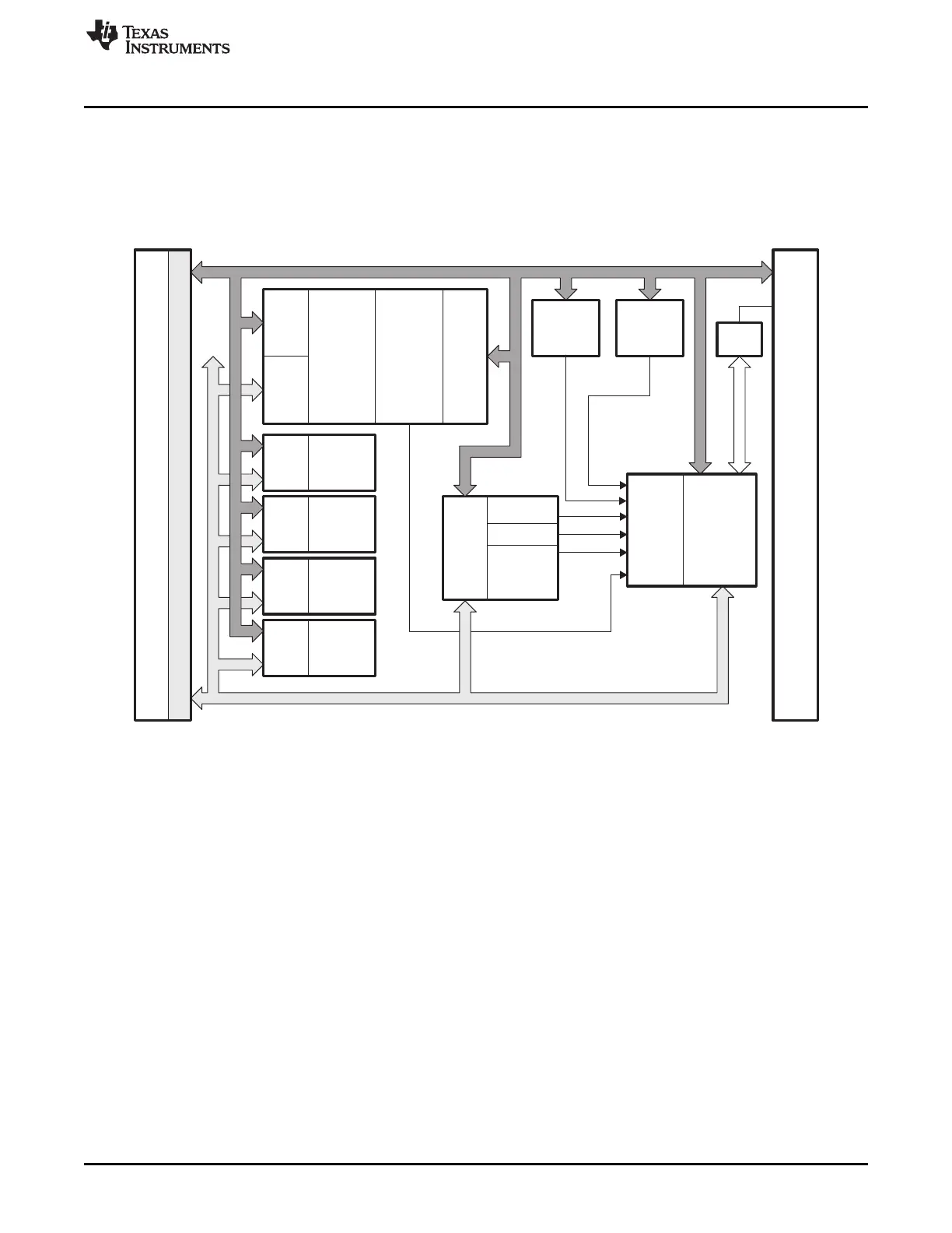
Figure 8-1 shows a device level block diagram of the DMA.
Figure 8-1. DMA Block Diagram
A The ePWM/HRPWM registers must be remapped to PF3 (through bit 0 of the MAPCNF register) before they can be
accessed by the DMA. The ePWM/HRPWM connection to DMA is not present in silicon revision 0.
 Loading...