GPBDAT
(latch)
GPBCLEAR
GPBTOGGLE
GPBQSEL1/2
Qual
GPBMUX1/2
SYSCLKOUT
GPIO34
to
GPIO63
Pins
PU
XRS
0 = Input , 1 = Output
Sync
XINT InputSignals
(XREADY,XD31:16_IN)
GPBDIR
(latch)
01
11
01
01
0x
1x
01
GPBCTRL
2
2
10
Perpheral1input
N/C
(defaultonreset)
(defaultonreset)
GPIOx_OUT
GPIOx_DIR
GPBPUD
0 = enablePU
1 = disablePU
(disabledafterreset)
async
(asyncdisable
whenlow)
0x
1x
11
10
XINTFOutputSignals
(XR/ , , ,
, /XA0,
XA7.1,XD31:16_OUT)
WXZCS0XZCS7
XWE0XWE1
N/C
N/C
Peripheral1output
Peripheral1outputenable
GPBSET
(defaultonreset)
3samples
6samples
00
00
00
00
XRS
DefaultatReset
XINTFOutputEnables
(XD_OEor1)
External
interrupt
MUX
GPIOXINT6SEL
GPIOXINT7SEL
GPIOXINT5SEL
GPIOXINT4SEL
GPIOXINT3SEL
PIE
GPBDAT (read)
High-
Impedance
Output
Control
General-Purpose Input/Output (GPIO)
www.ti.com
90
SPRUI07–March 2020
Submit Documentation Feedback
Copyright © 2020, Texas Instruments Incorporated
System Control and Interrupts
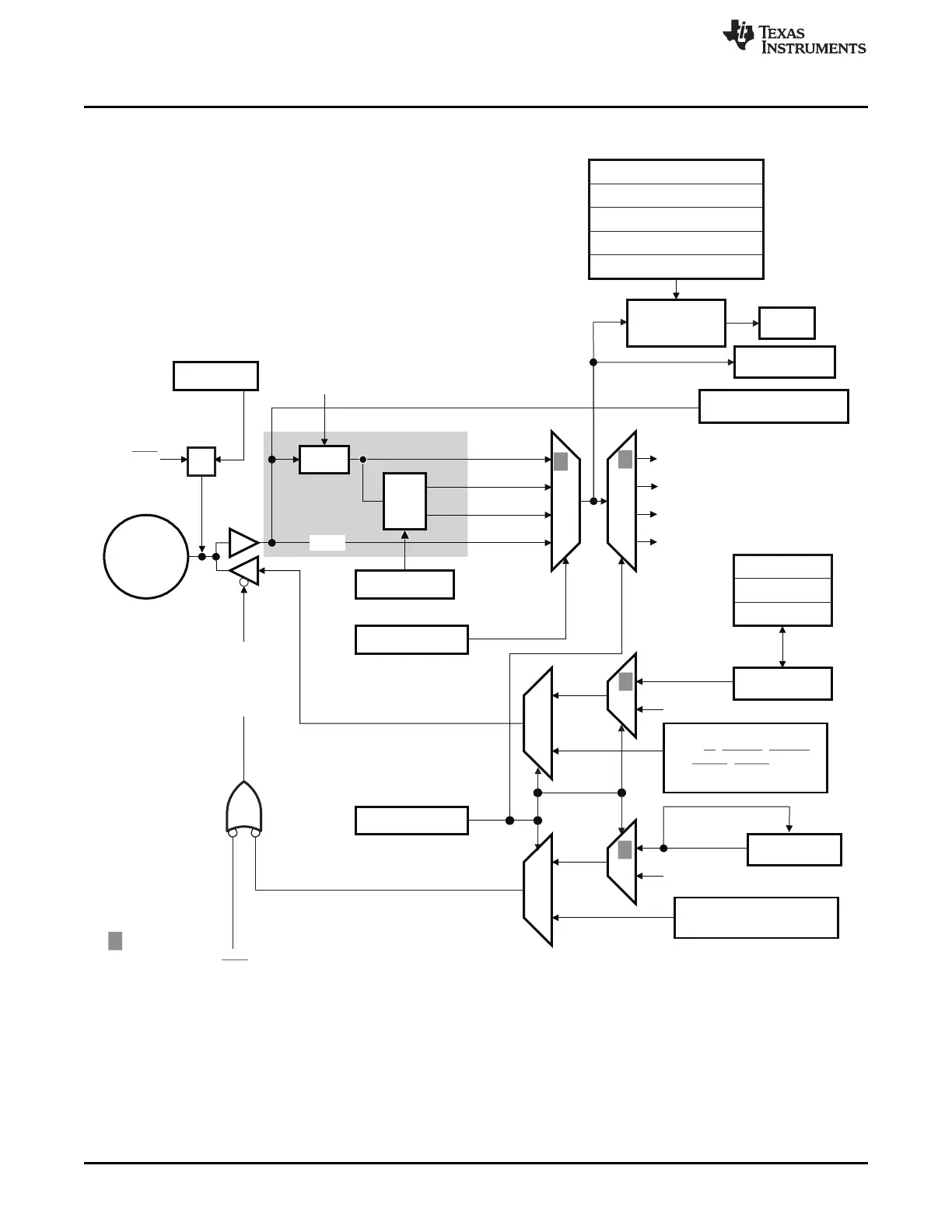
Figure 1-43. GPIO34 to GPIO63 Multiplexing Diagram (Peripheral 2 and Peripheral 3 Outputs Merged)
A The shaded area is disabled in the above GPIOs when the GPIOINENCLK bit is cleared to "0" in the PCLKCR3
register and the respective pin is configured as an output. This is to reduce power consumption when a pin is
configured as an output. Clearing the GPIOINCLK bit will reset the sync and qualification logic so no residual value is
left.
B The input qualification circuit is not reset when modes are changed (such as changing from output to input mode).
Any state will get flushed by the circuit eventually.
 Loading...