GPADAT
(latch)
GPACLEAR,
GPATOGGLE
GPAQSEL 1/2
Qual
GPAMUX 1/2
SYSCLKOUT
High
impedance
output
control
GPIO0
to
GPIO27
Pins
PU
XRS
Sync
Lowpower
modesblock
GPIOx.async
GPADIR
(latch)
01
11
01
GPACTRL
2
2
10
Peripheral1input
N/C
(defaultonreset)
(defaultonreset)
GPIOx_OUT
GPIOx_DIR
GPAPUD
0 = enablePU
1 = disablePU
(disabledafterreset)
async
(asyncdisable
whenlow)
11
10
Peripheral2input
Peripheral3input
Peripheral1output
GPASET,
(default
onreset)
3samples
6samples
00
00
XRS
(defaultonreset)
01
11
10
00
01
11
10
00
0=input,1=output
GPIOXINT1SEL
GPIOXINT2SEL
GPIOXNMISEL
External
interrupt
MUX
PIE
GPADAT (read)
GPIOLPMSEL
LPMCR0
Peripheral2output
Peripheral3output
Peripheral1outputenable
Peripheral2outputenable
Peripheral3outputenable
www.ti.com
General-Purpose Input/Output (GPIO)
87
SPRUI07–March 2020
Submit Documentation Feedback
Copyright © 2020, Texas Instruments Incorporated
System Control and Interrupts
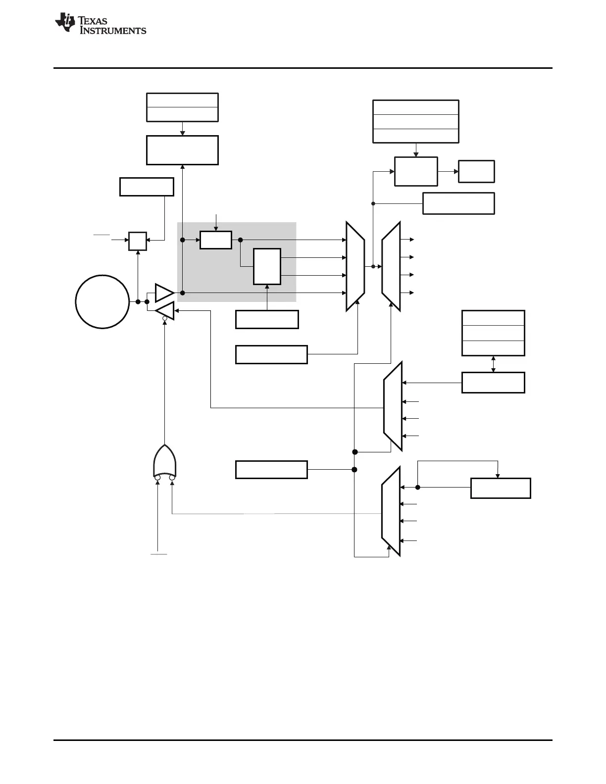
Figure 1-40. GPIO0 to GPIO27 Multiplexing Diagram
A The shaded area is disabled in the above GPIOs when the GPIOINENCLK bit is cleared to 0 in the PCLKCR3 register
and the respective pin is configured as an output. This is to reduce power consumption when a pin is configured as
an output. Clearing the GPIOINCLK bit will reset the sync and qualification logic so no residual value is left.
B GPxDAT latch/read are accessed at the same memory location.
 Loading...