RRDY
DR
FSR
CLKR
Read from DRR1(b)RBR1 to DRR1 copy(B)Read from DRR1(A)RBR1 to DRR1 copy(A)
C5C6C7B0B1B2B3B4B5B6B7A0A1
RBR[1,2] DRR[1,2]DRR[1,2]RBR[1,2]
To CPU or
DMA controller
justify and bit fill
or
PxWyBz = Phase x Word y Bit z
P2W12B0P2W12B1
MDRA
P1W1B15
P1W1B12
P1W1B13
P1W1B14
MFSRA
MCLKRA
1-bit data delay
McBSP Operation
www.ti.com
668
SPRUI07–March 2020
Submit Documentation Feedback
Copyright © 2020, Texas Instruments Incorporated
Multichannel Buffered Serial Port (McBSP)
Figure 12-12. Timing of an AC97-Standard Data Transfer Near Frame Synchronization
12.3.5 McBSP Reception
This section explains the fundamental process of reception in the McBSP. For details about how to
program the McBSP receiver, see Section 12.8.
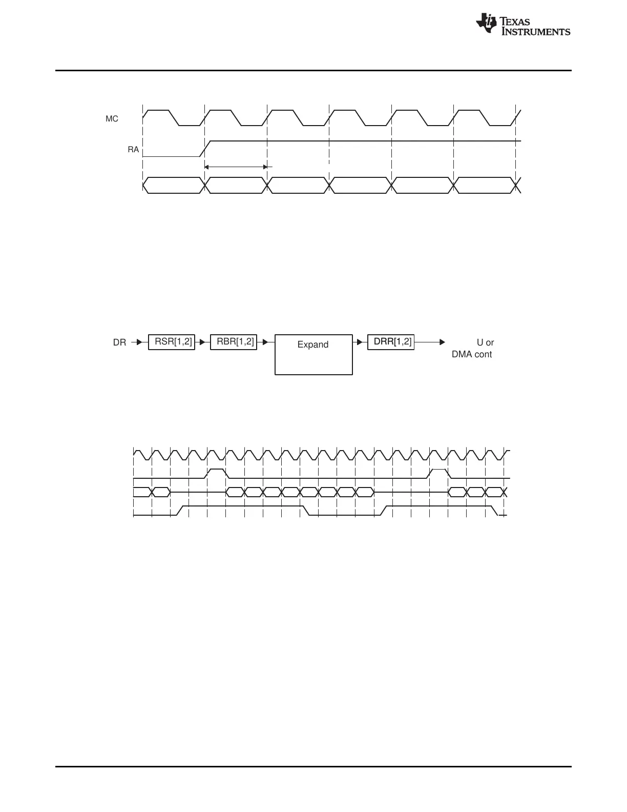
Figure 12-13 and Figure 12-14 show how reception occurs in the McBSP. Figure 12-13 shows the
physical path for the data. Figure 12-14 is a timing diagram showing signal activity for one possible
reception scenario. A description of the process follows the figures.
Figure 12-13. McBSP Reception Physical Data Path
A RSR[1,2]: Receive shift registers 1 and 2
B RBR[1,2]: Receive buffer registers 1 and 2
C DRR[1,2]: Data receive registers 1 and 2
Figure 12-14. McBSP Reception Signal Activity
A CLKR: Internal receive clock
B FSR: Internal receive frame-synchronization signal
C DR: Data on DR pin
D RRDY: Status of receiver ready bit (high is 1)
The following process describes how data travels from the DR pin to the CPU or to the DMA controller:
1. The McBSP waits for a receive frame-synchronization pulse on internal FSR.
2. When the pulse arrives, the McBSP inserts the appropriate data delay that is selected with the
RDATDLY bits of RCR2.
In the preceding timing diagram, a 1-bit data delay is selected.
3. The McBSP accepts data bits on the DR pin and shifts them into the receive shift register(s).
If the word length is 16 bits or smaller, only RSR1 is used. If the word length is larger than 16 bits,
RSR2 and RSR1 are used and RSR2 contains the most significant bits. For details on choosing a word
length, see Section 12.8.8, Set the Receive Word Length(s).
4. When a full word is received, the McBSP copies the contents of the receive shift register(s) to the
receive buffer register(s), provided that RBR1 is not full with previous data.
If the word length is 16 bits or smaller, only RBR1 is used. If the word length is larger than 16 bits,
 Loading...