Out
SRC
addr
(N)
Read
SRC
data
(N)
Out
DST
addr
(N)
Write
DST
data
(N)
Gen
SRC
addr
(N+1)
Gen
DST
addr
(N+1)
Gen
SRC
addr
(N+2)
Out
DST
addr
(N+1)
Write
DST
data
(N+1)
Gen
DST
addr
(N+2)
SYSCLK
Addrbus
Databus
Generate
address
Out
SRC
addr
(N+1)
Read
SRC
data
(N+1)
Out
SRC
addr
(N)
Read
SRC
data
(N)
Out
DST
addr
(N)
Out
SRC
addr
(N+1)
Write
DST
data
(N)
Gen
SRC
addr
(N+1)
Gen
DST
addr
(N+1)
Gen
SRC
addr
(N+2)
Read
SRC
data
(N+1)
Out
DST
addr
(N+1)
Out
SRC
addr
(N+2)
Write
DST
data
(N+1)
Gen
DST
addr
(N+2)
Gen
SRC
addr
(N+3)
Read
SRC
data
(N+2)
SYSCLK
Addrbus
Databus
Generate
address
Pipeline Timing and Throughput
www.ti.com
500
SPRUI07–March 2020
Submit Documentation Feedback
Copyright © 2020, Texas Instruments Incorporated
Direct Memory Access (DMA) Module
• ADC Memory Mapped Result Registers
• McBSP-A and McBSP-B Data Receive Registers (DRR2/DRR1) and Data Transmit Registers
(DXR2/DXR1)
• ePWM1-6/HRPWM1-6 Register when mapped to Peripheral Frame 3
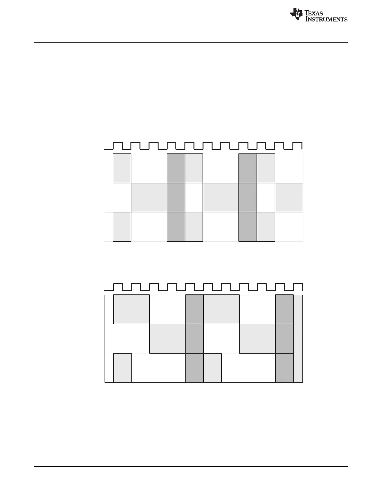
8.3 Pipeline Timing and Throughput
The DMA consists of a 4-stage pipeline as shown in Figure 8-3. The one exception to this is when a DMA
channel is configured to have one of the McBSPs as its data source. A read of a McBSP DRR register
stalls the DMA bus for one cycle during the read portion of the transfer, as shown in Figure 8-4.
Figure 8-3. 4-Stage Pipeline DMA Transfer
Figure 8-4. 4-Stage Pipeline With One Read Stall (McBSP as source)
In addition to the pipeline there are a few other behaviors of the DMA that affect it’s total throughput
• A 1-cycle delay is added at the beginning of each burst
• A 1-cycle delay is added when returning from a CH1 high priority interrupt
• 32-bit transfers run at double the speed of a 16-bit transfer (i.e., it takes the same amount of time to
transfer a 32-bit word as it does a 16-bit word)
• Collisions with the CPU may add delay slots (see Section 8.4)
 Loading...