Cortex-M3 Processor (Reference Material)
UG0331 User Guide Revision 15.0 94
3.7 Cortex-M3 Processor Peripherals
The following sections are the reference material for the Cortex-M3 processor core peripherals
descriptions in this user guide.
3.7.1 About the Cortex-M3 Processor Peripherals
The following table provides the address map of the Private peripheral bus (PPB).
In register descriptions:
• the register type is described as follows:
• RW: Read and write.
• RO: Read-only.
• WO: Write-only.
•the required privilege gives the privilege level required to access the register, as follows:
• Privileged: Only privileged software can access the register.
• Unprivileged: Both unprivileged and privileged software can access the register.
3.7.1.1 Nested Vectored Interrupt Controller
This section describes the Nested Vectored Interrupt Controller (NVIC) and the registers it uses. The
NVIC supports:
• 1 to 240 interrupts.
• A programmable priority level of 0-255 for each interrupt. A higher level corresponds to a lower
priority, so level 0 is the highest interrupt priority.
• Level and pulse detection of interrupt signals.
• Dynamic reprioritization of interrupts.
• Grouping of priority values into group priority and subpriority fields.
• Interrupt tail-chaining.
• An external Non-maskable interrupt (NMI).
The processor automatically stacks its state on exception entry and unstacks this state on exception exit,
with no instruction overhead. This provides low latency exception handling. The hardware
implementation of the NVIC registers is:
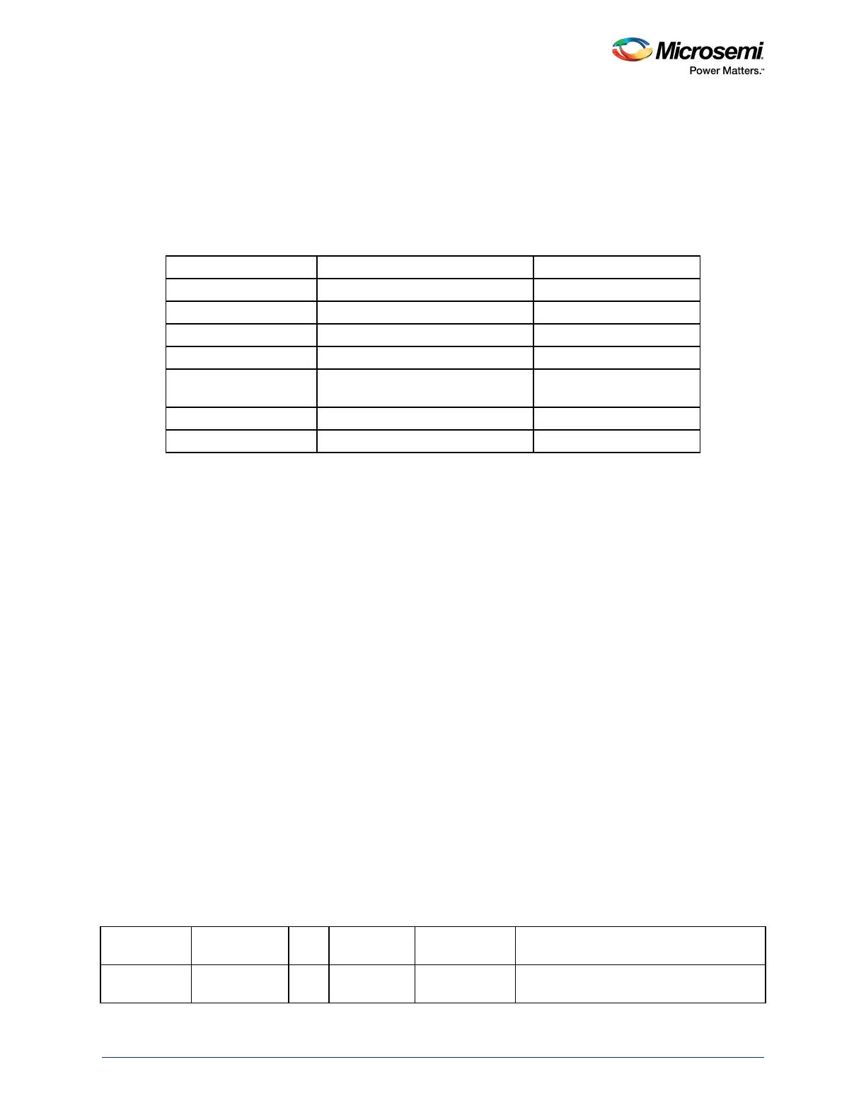
Table 39 • Core Peripheral Register Regions
Address Core Peripheral See
0xE000E008
-
0xE000E00F
System control block Tab le 50 , page 102
0xE000E010
-
0xE000E01F
System timer Tab le 71 , page 119
0xE000E100
-
0xE000E4EF
Nested Vectored Interrupt Controller Ta ble 4 0, page 95
0xE000ED00
-
0xE000ED3F
System control block Tab le 50 , page 102
0xE000ED90
-
0xE000ED93
MPU Type Register Reads as zero, indicating no
MPU is implemented
1
1. Software can read the MPU Type Register at
0xE000ED90
to test for the presence of a memory
protection unit (MPU).
0xE000ED90
-
0xE000EDB8
Memory protection unit Tab l e 77 , page 123
0xE000EF00
-
0xE000EF03
Nested Vectored Interrupt Controller Ta ble 4 0, page 95
Table 40 • NVIC Register Summary
Address Name Type
Required
privilege
Reset
value See
0xE000E100
-
0xE000E11C
NVIC_ISER0-
NVIC_ISER7
RW Privileged 0x00000000 Interrupt Set-enable Registers, page 96