System Register Block
UG0331 User Guide Revision 15.0 676
22.1.3 Locking and Unlocking a Register
A register can be locked or unlocked by setting the appropriate lock bit value in the lock bit configuration
.txt file.
1. Browse to locate the lock bit configuration
.txt file.
2. Do one or both of the following:
• Set the lock bit value to 0 for the registers you want to lock.
• Set the lock bit value to 1 for the registers you want to unlock.
3. Save the file, and import the file into the project (Design Flow window > Configure Register Lock
Bits), see Figure 317, page 674.
4. Regenerate the bitstream.
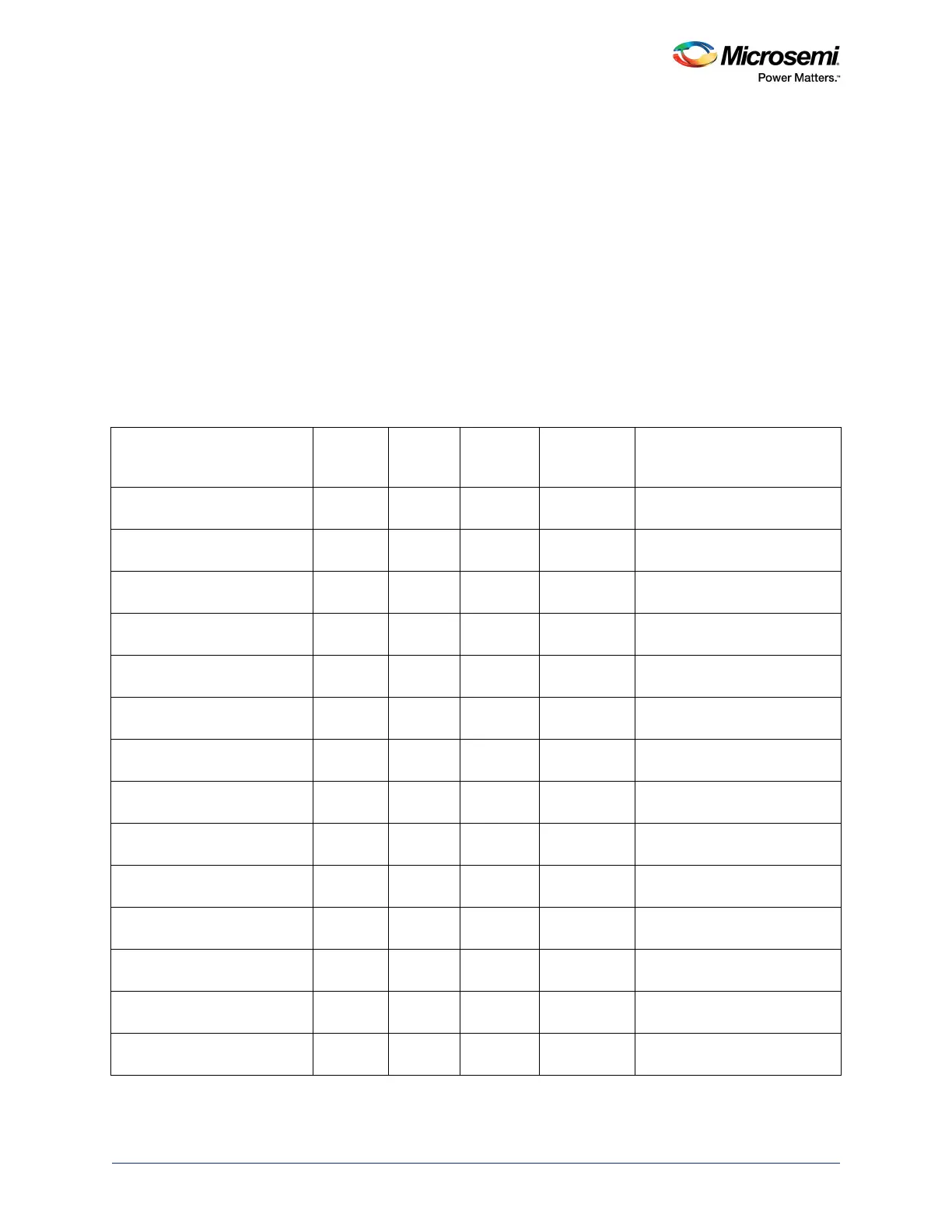
22.2 Register Map
The following table lists all the registers in the SYSREG block. The SYSREG block is located at address
0x40038000 in Cortex-M3 processor address space.
Table 650 • SYSREG
Register Name
Addr.
Offset
Register
Type
Flash
Write
Protect Reset Source Description
ESRAM_CR 0x0 RW-P Register SYSRESET_
N
Controls address mapping of
the eSRAMs
ESRAM_MAX_LAT 0x4 RW-P Register SYSRESET_
N
eSRAM0 and eSRAM1
maximum latency
DDR_CR 0x8 RW-P Register SYSRESET_
N
DDR Configuration Register
ENVM_CR 0XC RW-P Register SYSRESET_
N
eNVM Configuration Register
ENVM_REMAP_BASE_CR 0x10 RW-P Register SYSRESET_
N
eNVM Remap Base Address
Control Register
ENVM_REMAP_FAB_CR 0x14 RW-P Register SYSRESET_
N
eNVM Remap Base Address
Control Register
CC_CR 0x18 RW-P Register SYSRESET_
N
Used to configure cache
CC_REGION_CR 0x1C RW-P Register SYSRESET_
N
Cache Region Control Register
CC_LOCK_BASE_ADDR_CR 0x20 RW-P Register SYSRESET_
N
Cache Lock Base Address
Control Register
CC_FLUSH_INDX_CR 0x24 RW-P Register SYSRESET_
N
Cache Flush Index Control
Register
DDRB_BUF_TIMER_CR 0x28 RW-P Register SYSRESET_
N
DDR write buffer timeout
DDRB_NB_ADDR_CR 0x2C RW-P Register SYSRESET_
N
DDR non-bufferable address
region base address
DDRB_NB_SIZE_CR 0x30 RW-P Register SYSRESET_
N
Size of non- bufferable address
region
DDRB_CR 0x34 RW-P Register SYSRESET_
N
MSS DDR bridge Configuration
Register