Cortex-M3 Processor Overview and Debug Features
UG0331 User Guide Revision 15.0 7
• Not all registers in the register bank are reset
• Endianness: little endian only
• Auxiliary control register is included
• Wake-up interrupt controller (WIC) is not included
For more details of these configurations and optional features, refer to Cortex-M3 Processor (Reference
Material), page 18.
2.2 Functional Description
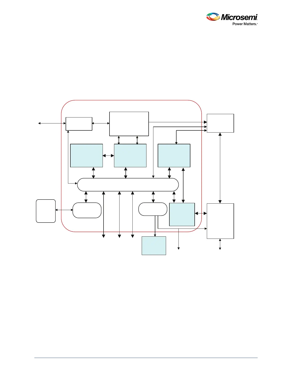
The following figure shows the Cortex-M3 processor, core peripherals and debug subsystem
implementations used in SmartFusion2.
Figure 1 • Cortex-M3 Processor R2P1 Block Diagram as Implemented in the SmartFusion2 SoC FPGA
The following topics are covered in detail in the sub-sections:
• Cortex-M3 Processor NVIC
• Cortex-M3 Processor SysTick Timer
• Cortex-M3 Processor Debug Subsystem
• Data Watch Point (DWP) and Trace
• Instrumentation Trace Macrocell
• Embedded Trace Macrocell
Note: The Cortex-M3 operating frequency is dependent on device speed grade (up to 166 MHz). Refer to
SmartFusion2 Specifications-MSS Clock Frequency section from DS0128: IGLOO2 FPGA and
SmartFusion2 SoC FPGA Datasheet for more information.
Core
ETM
Data Watchpoint
Trace
(DWT)
Trace Port
Interface Unit
(TPIU)
AHB
Access Port
(AHB- AP)
Cortex - M3
Processor
Debug
(Serial Wire
or JTAG)
Trigger
Cortex- M 3 Processor
CPU I/F
Nested Vector
Interrupt
Controller (NVIC)
Flash Patch Br eak Point
( FPB )
Memory Protection Unit
(MPU )
Instrumentation
Trace Macrocell
(ITM)
APB I /F
CoreSight
ROM Table
Private
Peripheral
Bus
I-Code
Bus
D -Code
Bus
System
Bus
Interrupts and
Power Control
Instruction Data
Trace Port
Interface
AHB Bus Matrix
Cortex- M3 Processor