Cortex-M3 Processor (Reference Material)
UG0331 User Guide Revision 15.0 31
The Code, SRAM, and external RAM regions can hold programs. However, ARM recommends that
programs always use the Code region. This is because the processor has separate buses that enable
instruction fetches and data accesses to occur simultaneously.
The MPU can override the default memory access behavior described in this section. For more
information, see Memory Protection Unit, page 20.
3.5.2.3.1 Additional memory access constraints for caches and shared memory
When a system includes caches or shared memory, some memory regions have additional access
constraints, and some regions are subdivided, as detailed in the following table.
3.5.2.3.2 Instruction Prefetch and Branch Prediction
The Cortex-M3 processor:
• Prefetches instructions ahead of execution
• Speculatively prefetches from branch target addresses.
3.5.2.4 Software Ordering of Memory Accesses
The order of instructions in the program flow does not always guarantee the order of the corresponding
memory transactions. This is because:
• the processor can reorder some memory accesses to improve efficiency, providing this does not
affect the behavior of the instruction sequence.
• the processor has multiple bus interfaces
• memory or devices in the memory map have different wait states
• some memory accesses are buffered or speculative.
0xE0000000-
0xE00FFFFF
Private Peripheral
Bus
Strongly-
ordered
XN This region includes the NVIC, System timer, and
system control block.
0xE0100000-
0xFFFFFFFF
Vendor specific Device XN Accesses to this region are to vendor-specific
peripherals.
1. See Memory Regions, Types and Attributes, page 29 for more information.
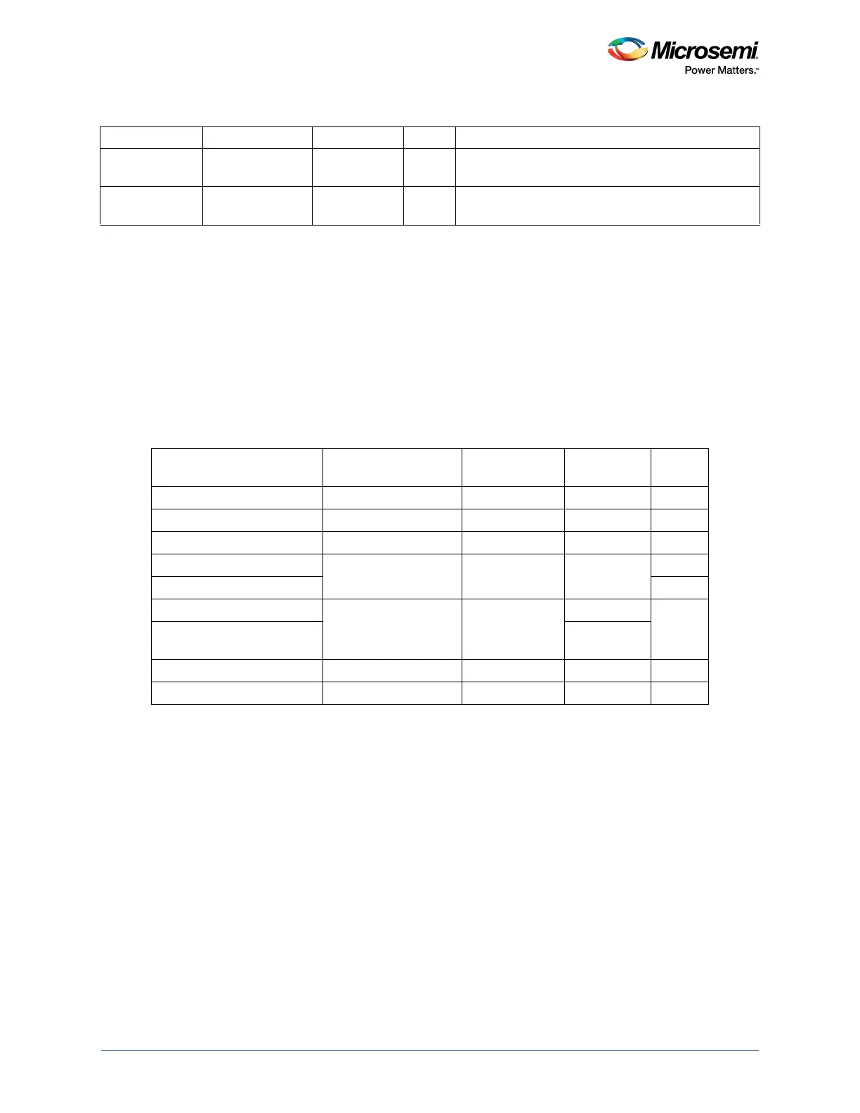
Table 18 • Memory Region Shareability and Cache Policies
Address range Memory region Memory type
1
1. See Memory Regions, Types and Attributes, page 29 for more information.
Shareability
Cache
policy
2
2. WT = Write through, no write allocate. WBWA = Write back, write allocate.
0x00000000- 0x1FFFFFFF Code Normal WT
0x20000000- 0x3FFFFFFF SRAM Normal WBWA
0x40000000- 0x5FFFFFFF Peripheral Device
0x60000000- 0x7FFFFFFF External RAM Normal WBWA
0x80000000- 0x9FFFFFFF WT
0xA0000000- 0xBFFFFFFF External device Device Shareable
0xC0000000- 0xDFFFFFFF Non-
shareable
0xE0000000- 0xE00FFFFF Private Peripheral Bus Strongly- ordered Shareable
0xE0100000- 0xFFFFFFFF Vendor-specific device Device
Table 17 • Memory Access Behavior (continued)
Address range Memory region Memory Type
1
XN
1
Description