Cortex-M3 Processor (Reference Material)
UG0331 User Guide Revision 15.0 34
3.5.2.5.2 Directly accessing a bit-band region
Behavior of Memory Accesses, page 30 describes the behavior of direct byte, halfword, or word
accesses to the bit-band regions.
3.5.2.6 Memory Endianness
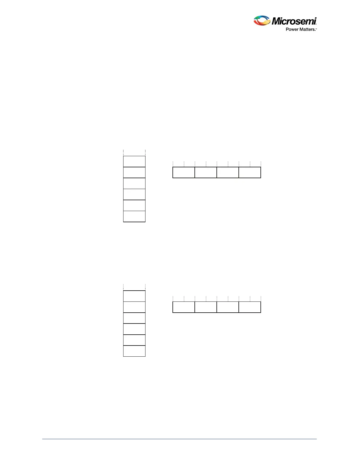
The processor views memory as a linear collection of bytes numbered in ascending order from zero. For
example, bytes 0-3 hold the first stored word, and bytes 4-7 hold the second stored word. Byte-invariant
big-endian format or Little-endian format describes how words of data are stored in memory.
3.5.2.6.1 Byte-invariant Big-endian Format
In byte-invariant big-endian format, the processor stores the most significant byte of a word at the lowest-
numbered byte, and the least significant byte at the highest-numbered byte. The following illustration
shows the byte-invariant big-endian format.
Figure 14 • Byte-Invariant Big-Endian Format
3.5.2.6.2 Little-Endian format
In little-endian format, the processor stores the least significant byte of a word at the lowest-numbered
byte, and the most significant byte at the highest-numbered byte. Cortex-M3 processor configured for
SmartFusion2 SoC FPGA MSS uses only little endian. The following figure illustrates the little-endian
format.
Figure 15 • Little Endian Format
3.5.2.7 Synchronization Primitives
The Cortex-M3 processor instruction set includes pairs of synchronization primitives. These provide a
non-blocking mechanism that a thread or process can use to obtain exclusive access to a memory
location. Software can use them to perform a guaranteed read-modify-write memory update sequence,
or for a semaphore mechanism.
A pair of synchronization primitives comprises:
Memory Register
Address A
A+1
msbyte
lsbyte
A+2
A+3
07
B3B2B0 B1
31 24 23 16 15 8 7 0
B0
B1
B2
B3
Memory Register
Address A
A+1
lsbyte
msbyte
A+2
A+3
07
B0B1B3 B2
31 24 23 16 15 8 7 0
B0
B1
B2
B3