System Register Block
UG0331 User Guide Revision 15.0 684
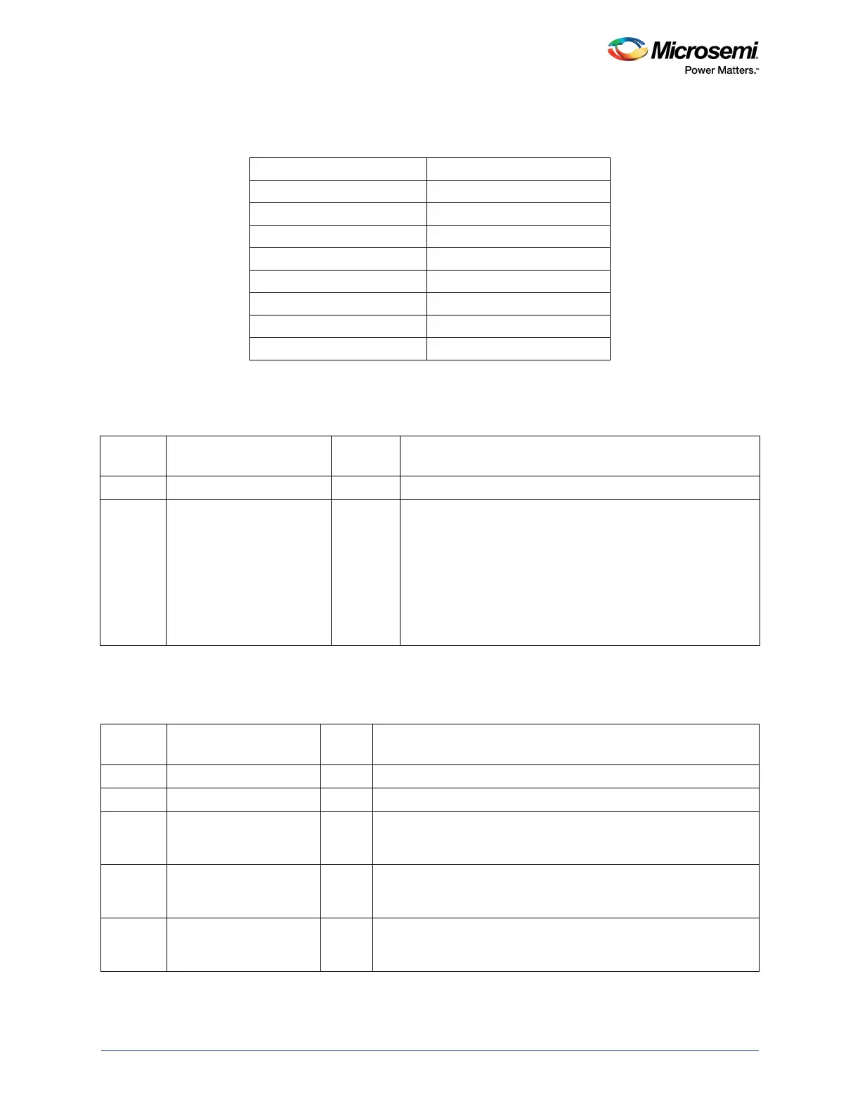
The following table lists eSRAM maximum latency values, where x is either 0 or 1.
22.3.4 DDR Configuration Register
22.3.5 eNVM Configuration Register
Table 654 • eSRAM Maximum Latency Values
SW_MAX_LAT_ESRAM<X> Latency
0 8 (default)
11
22
33
44
55
66
77
Table 655 • DDR_CR
Bit
Number Name
Reset
Value Description
[31:1] Reserved 0
0 SW_CC_DDRFWREMAP 0 Indicates that DDR_Space0 and DDR_Space1 are remapped to
the lCODE/DCODE space of the Cortex-M3 processor. Both
DDR spaces also remain visible in the SYSTEM space of the
Cortex-M3 processor and remain visible at this location to all
other non-Cortex-M3 processor masters. The bit definitions:
0: No DDR space remap is enabled. This means that eNVM is
present at location 0x00000000.
1: DDR_Space0 and DDR_Space1 are remapped to location
0x00000000 of Cortex-M3 processor ICODE/DCODE space.
Table 656 • ENVM_CR
Bit
Number Name
Reset
Value Description
[31:17] Reserved 0
16 ENVM_SENSE_ON 0 Turns on or off the sense amps for both NVM0 and NVM1
15 ENVM_PERSIST 0 Reset control for NVM0 and NVM1
0: Reset on SYSRESET_N and PORESET_N
1: Reset on PORESET_N
14 NV_DPD1 0 Deep power-down control for the NVM1
0: Normal operation
1: NVM deep power-down
13 NV_DPD0 0 Deep power-down control for the NVM0
0: Normal operation
1: NVM deep power-down