Reset Controller
UG0331 User Guide Revision 15.0 651
21.2.3 DEVRST_N Power-Up to Functional Time
This scenario provides power-up to functional time data with respect to DEVRST_N when the FPGA
fabric, the FPGA I/O, and external oscillator are used. The design setup is same as the VDD power-up to
functional time, as shown in the following figure.
Note: It is not recommended to assert DEVRST_N pin during programming (including eNVM), as it corrupts the
device configuration. For more information on proper usage of the DEVRST_N pin,
see the AC393: Board Design Guidelines for SmartFusion2 SoC and IGLOO2 FPGAs Application Note.
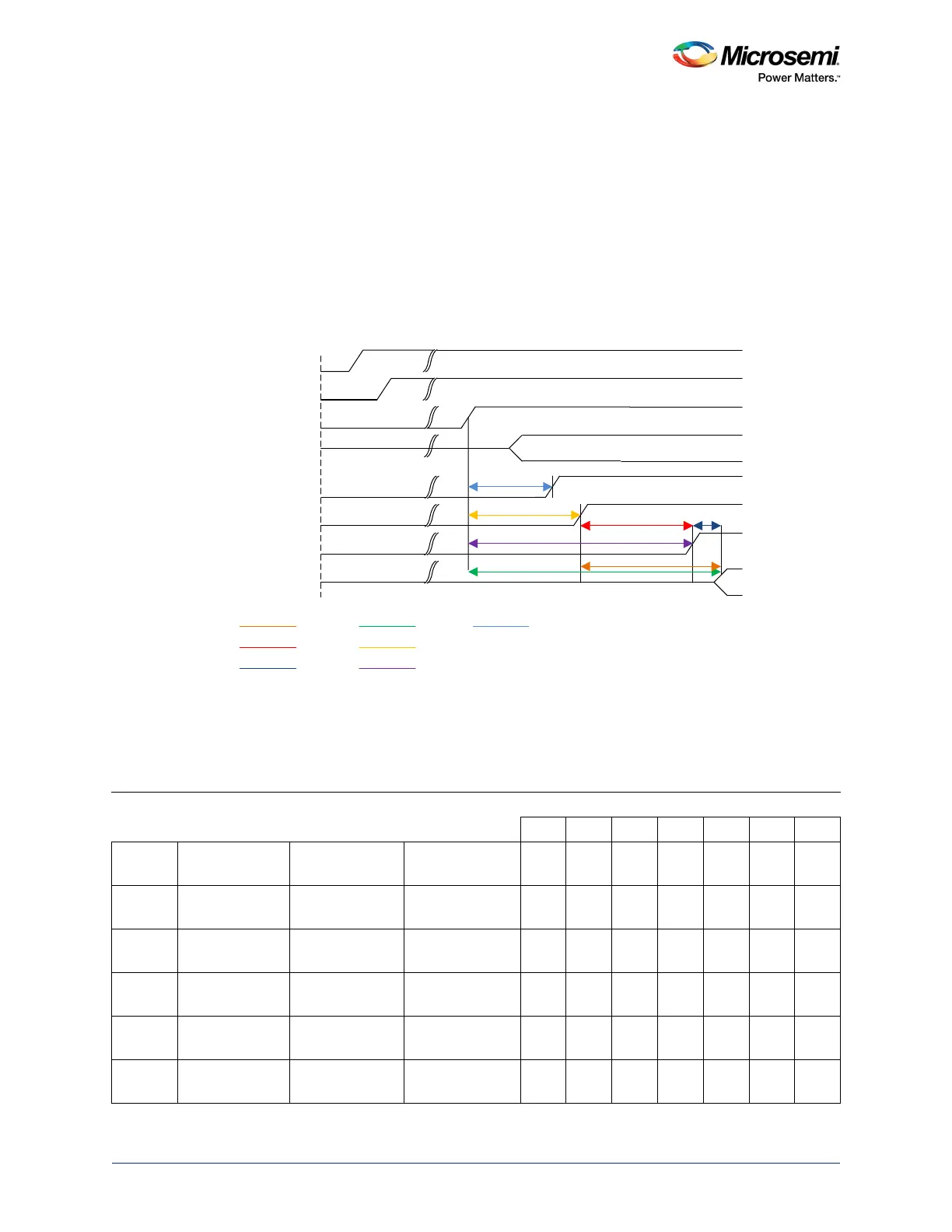
The following figure shows the behavior of different signals when DEVRST_N is asserted and MSS is
used with VDD = 1.2 V, VDDI = 2.5 V, and Tj = 25 °C.
Figure 283 • DEVRST_N Power-Up to Functional Timing
The following table lists power-up to functional time of M2S005, M2S010, M2S025, M2S050, M2S060,
M2S090, and M2S150 devices with MSS clock ranging from 3 MHz to 166 MHz.
Note: The timing numbers shown in the below table is for worst case condition.
Table 646 • DEVRST_N Power-Up to Functional Time
Test
Case Start Point End Point Description
Power-Up to Functional Time (µs)
005 010 025 050 060 090 150
Case1 POWER_ON_
RESET_N
Output available
at I/O
Fabric to output 518 501 527 521 422 419 694
Case 2 POWER_ON_
RESET_N
MSS_RESET_N
_ M2F
Fabric to MSS 515 497 524 518 417 414 689
Case 3 MSS_RESET_
N_M2F
Output available
at I/O
MSS to output 3.5 3.5 3.5 3.3 4.8 4.8 4.8
Case 4 DEVRST_N Output available
at I/O
DEVRST_N to
output
706 768 715 691 641 635 871
Case 5 DEVRST_N POWER_ON_
RESET_N
DEVRST_N to
fabric
234 289 216 213 237 234 219
Case 6 DEVRST_N MSS_RESET_N
_ M2F
DEVRST_N to
MSS
702 765 712 688 636 630 866
9''9339'',[
5&26&B0+]
'(9567B1
,1%8)
,1%8):($.38//
06,206,2'''5,2
32:(5B21B5(6(7B1
066B5(6(7B1B0)
287%8)
V
V
V
V
V
V
V
&DVH
&DVH
&DVH
&DVH
&DVH
&DVH
06
+LJK=
7ULVWDWH
+LJK=
7ULVWDWH
&DVH