Cache Controller
UG0331 User Guide Revision 15.0 133
4 Cache Controller
The SmartFusion2 SoC FPGA has an instruction cache. The ARM
®
Cortex
®
-M3 processor interfaces to
this instruction cache through the Cache Controller. The Cache Controller treats embedded SRAM
(eSRAM), embedded nonvolatile memory (eNVM), or DDR memory as main memory.
4.1 Features
• 8 KB of cache size
• Four-way set associativity: Cache Controller has a four-way set associative cache subsystem with
32 byte cache lines organized as 64 sets of 4 cache lines, with a total of 256 locations.
• Cache line size is 32 bytes, fixed irrespective of DDR burst.
• Least recently used (LRU) cache line replacement policy.
• Fill mechanism: Full cache line refill and critical word first.
• The Cortex-M3 processor can write to Cache Memory through the System bus (SBUS).
• Zero wait state in case of a hit (instruction in Cache Memory) and can run up to the maximum
system frequency.
• Supports Cache locked mode
• Cache is constructed of latches
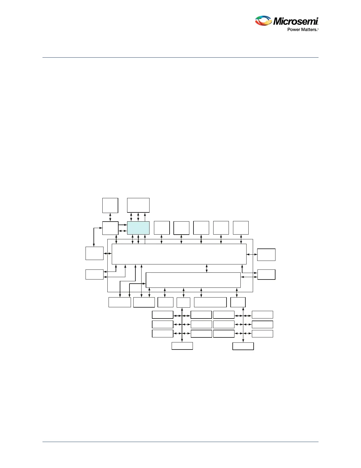
The following figure depicts the connectivity of the Cache Controller in a SmartFusion2 device.
Figure 56 • Cache Controller Interfaces to Cortex-M3 Processor, AHB Bus Matrix, and MDDR Bridge
AHB Bus Matrix
eSRAM_0
System
Controller
Cache
Controller
SD IC
ARM Cortex-M3
Processor
SDI
MSS DDR
Bridge
PDMA
MS6
MM3
AHB To AHB Bridge with Address Decoder
USB OTG
HPDMA
MDDR
APB_0
SYSREG
Triple Speed
Ethernet MAC
FIC_0
MM4 MS4
MS2 MS3 MS0
MS5
MS1
MM5 MM6
MM7
MM8
MM2 MM1 MM0 MM9
IDC
D/S
eNVM_0 eNVM_1 eSRAM_1
FIC_2 (Peripheral
Initialization)
APB_1
MMUART_0
SPI_0
I2C_0
PDMA
Configuration
WATCHDOG
FIIC
TIMERx2
MMUART_1
SPI_1
I2C_1
GPIO
CAN
RTC
COMM_BLK
FIC_1
MSS_FIC
MS6_USB
MS5_MAC MS5_SR MS5_APB0 MS5_FIC2 MS5_APB1