Inter-Integrated Circuit Peripherals
UG0331 User Guide Revision 15.0 550
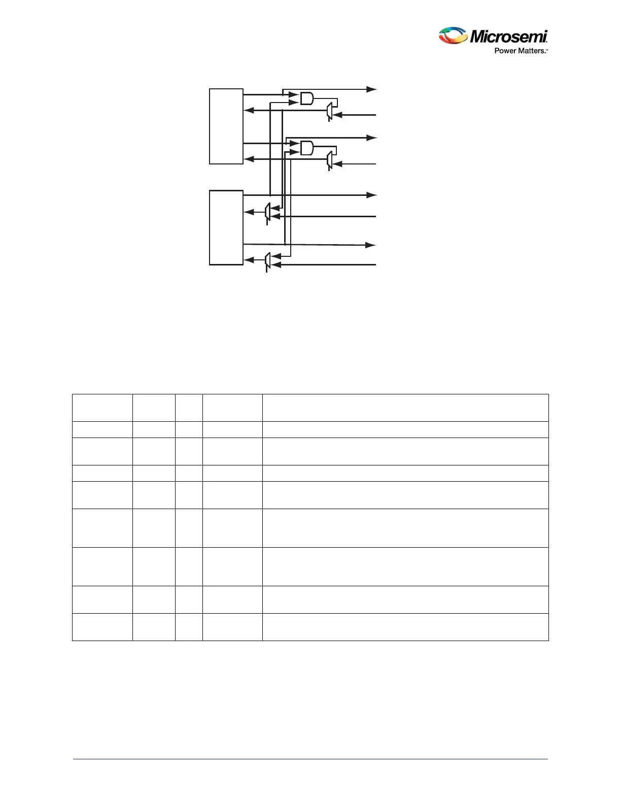
Figure 238 • I
2
C Loopback Block Diagram
15.4 I
2
C Register Map
The internal register address map and reset values of each APB accessible register for I
2
C peripherals
are listed in the following table. The I2C_0 base address resides at 0x40002000 and extends to address
0x40002FFF in the Cortex-M3 processor memory map. The I2C_1 base address resides at 0x40012000
and extends to address 0x40012FFF in the Cortex-M3 processor memory map.
Table 520 • I
2
C Register Map
Register
Name
Address
Offset R/W Reset Value Description
CTRL 0x00 R/W 0x00 Control register: Used to configure the I
2
C peripheral.
STATUS 0x04 R 0xF8 Status register: Read-only value which indicates the current state of
the I
2
C peripheral.
DATA 0x08 R/W 0x00 Data register: Read/write data to/from the serial interface.
SLAVE0 ADR 0x0C R/W 0x00 Slave0 address register: Contains the primary programmable address
of the I
2
C peripheral.
SMBUS 0x10 R/W 0b01X1X000 SMBus register: Configuration register for SMBus timeout reset
condition and for the optional SMBus signals SMBALERT_N and
SMSBUS_N.
FREQ 0x14 R/W 0x08 Frequency register: Necessary for configuring real-time timeout logic.
Can be set to the PCLK frequency for 25 ms SMBus timeouts, or the
timeout value maybe increased/decreased.
GLITCHREG 0x18 R/W 0x03 Glitch Reg length register: Used to adjust the input glitch filter length. If
GLITCHREG_FIXED = 0, then the register can be set from 3 to 21.
SLAVE1 ADR 0x1C R/W 0x00 Slave1 address register: Contains the secondary programmable
address of the I
2
C peripheral.
I2C_0
I2C_1
SCL 0
SCL 1
SDA 0
SDA 1
SCL 0
SCL 1
SDA 0
SDA 1
SCL OUT
SCL IN
SDA OUT
SDA IN
SCL OUT
SCL IN
SDA OUT
SDA IN
MSS_I2CLOOPBACK bit
MSS_I2CLOOPBACK bit
MSS_I2CLOOPBACK bit
MSS_I2CLOOPBACK bit