Serial Peripheral Interface Controller
UG0331 User Guide Revision 15.0 527
Refer to the In-Application Programming chapter of UG0451: IGLOO2 and SmartFusion2
Programming User Guide for more information on usage of SPI_0 peripheral in IAP.
14.4 SPI Register Map
This section provides SPI registers along with the address offset, functionality, and bit definitions.
14.4.1 SYSREG Configuration Register Summary
The registers listed in the following table control the behavior of the SPI peripherals. Refer to the System
Register Block, page 670 for a detailed description of each register and bit.
14.4.2 SPI Register Summary
The following table summarizes each of the SPI registers described in this document. The SPI_0 base
address resides at 0x40001000 and extends to address 0x40001FFF in the Cortex-M3 processor
memory map. The SPI_1 base address resides at 0x40011000 and extends to address 0x40011FFF in
the Cortex-M3 processor memory map.
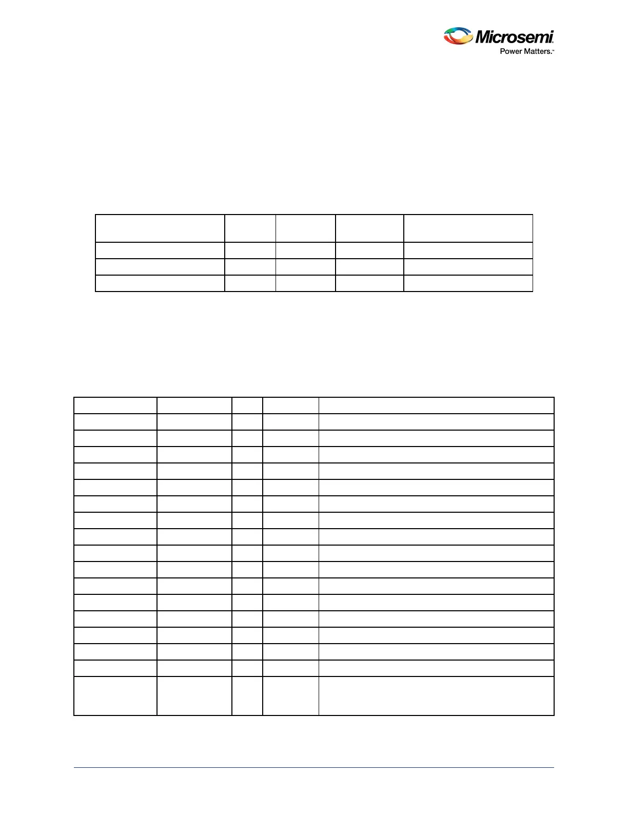
Table 498 • SYSREG Control Registers
Register Name
Register
Type
Flash Writer
Protect Reset Source Description
SOFT_RESET_CR RW-P Bit SYSRESET_N Soft reset control
LOOPBACK_CR RW-P Register SYSRESET_N Loop back control
PERIPH_CLK_MUX_SEL_CR RW-P Register PORESET_N Peripheral clock MUX select
Table 499 • SPI Register Summary
Register Name Address Offset R/W Reset Value Description
CONTROL 0x00 R/W 0x80000102 Control register
TXRXDF_SIZE 0x04 R/W 0x04 Transmit and receive data frame size
Status 0x08 R 0x2440 Status register
INT_CLEAR 0x0C W 0x0 Interrupt clear register
RX_DATA 0x10 R 0x0 Receive data register
TX_DATA 0x14 W 0x0 Transmit data register
CLK_GEN 0x18 R/W 0x07 Output clock generator (master mode)
SLAVE_SELECT 0x1C R/W 0x0 Specifies slave selected (master mode)
MIS 0x20 R 0x0 Masked interrupt status
RIS 0x24 R 0x0 Raw interrupt status
CONTROL2 0x28 R/W 0x0 Control bits for enhanced modes
COMMAND 0x2C R/W 0x0 Command register
PKTSIZE 0x30 R/W 0x0 Packet size
CMD_SIZE 0x34 R/W 0x0 Command size
HWSTATUS 0x38 R/W 0x0 Slave hardware status
STAT8 0x3C R 0x44 Status register
CTRL0 0x40 R/W 0x02 Aliased CONTROL register bits 7:0. This register allows
byte operations from an 8-bit processor in the fabric. It is
not intended for access from internal MSS masters.