RTC System
UG0331 User Guide Revision 15.0 613
Refer to Table 605, page 609 for register bit allocation.
18.5 SYSREG Control Registers
The RTC_WAKEUP_CR in the SYSREG block provides masking for the RTC_WAKEUP interrupt to the
fabric, the Cortex-M3 processor, and the system controller. Refer to the System Register Block, page 670
for bit details.
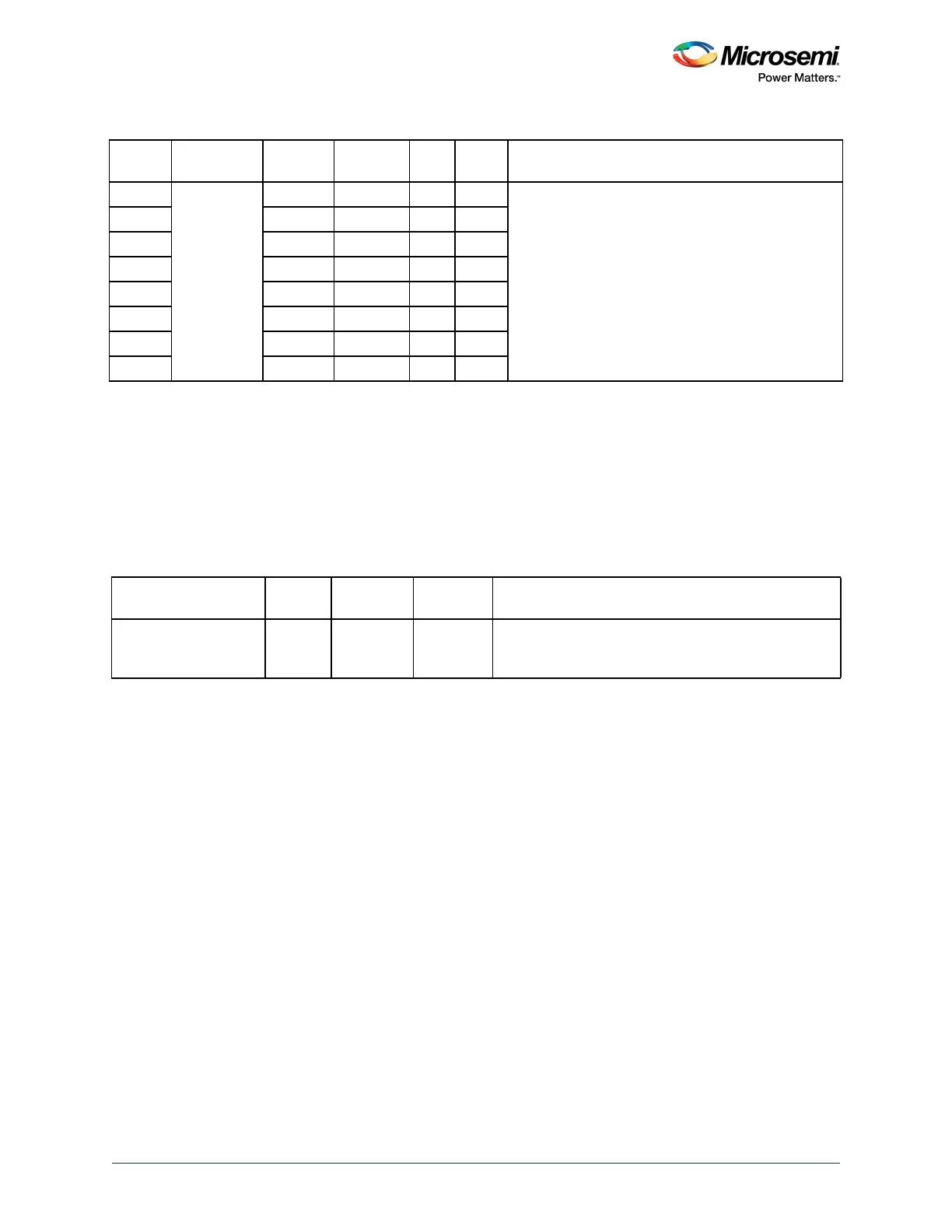
0x50 Date/Time
Direct Byte
Mode
[5:0] Seconds R/W 0 Direct mode returns the date/time at the point that
each of the the reads take place. Allows the
individual byte of the date and timer to be read. Each
read returns the current date/time value. It is possible
that the date/time may increment between reads.
For writing all fields (0 × 50 - × 6C) must be written.
The control register upload bit uploads data to the
RTC.
These registers are for use when clock_mode = 1.
0x54 [5:0] Minutes R/W 0
0x58 [4:0] Hours R/W 0
0x5C [4:0] Day R/W 0
0x60 [4:0] Month R/W 0
0x64 [7:0] Year R/W 0
0x68 [2:0] Weekday R/W 0
0x6C [5:0] Week R/W 0
Table 612 • The RTC_WAKEUP_CR in the SYSREG Block
Register Name
Register
Type
Flash Write
Protect
Reset
Source Description
RTC_WAKEUP_CR RW-P Register sysreset_n Provides masking for the RTC_WAKEUP interrupt to
the fabric, the Cortex-M3 processor, and the system
controller.
Table 611 • Date and Time (continued)
Address
Offset
Register
Name
Bit
Numbers Name R/W
Reset
Value Description