Serial Peripheral Interface Controller
UG0331 User Guide Revision 15.0 531
14.4.3.4 SPI Interrupt Clear Register (INT_CLEAR)
The following table describes the Interrupt Clear register. A read to this register has no effect. It returns
all zeroes.
14.4.3.5 SPI Receive Data Register (RX_DATA)
The following table describes the Receive Data register.
14.4.3.6 SPI Transmit Data Register (TX_DATA)
The following table describes the Transmit Data register.
14.4.3.7 SPI SCLK Generation Register (CLK_GEN)
The following table describes the clock modes used to calculate the SPICLK divider. Table 507, page 532
describes the SPICLK rates in different modes.
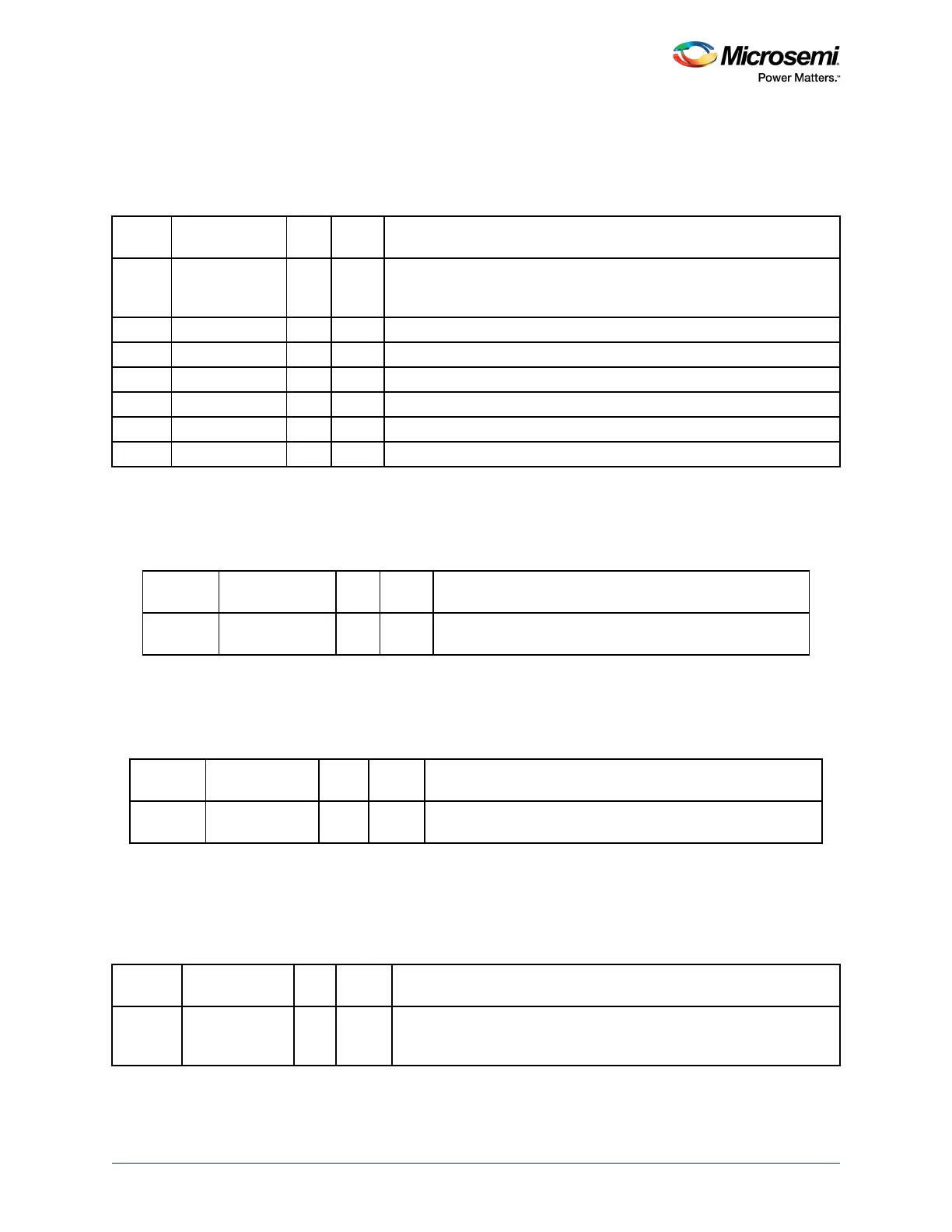
Table 503 • INT_CLEAR
Bit
Number Name R/W
Reset
Value Description
[31:6] Reserved W 0 Software should not rely on the value of a reserved bit. To provide
compatibility with future products, the value of a reserved bit should be
preserved across a read-modify-write operation.
5 SSEND W Write one to clear the interrupt
4 CMDINT W Write one to clear the interrupt
3 TXCHUNDRUN W 0 Transmit channel under-run
2 RXCHOVRFLW W 0 Receive channel over flow
1 RXRDYCLR W 0 Clears receive ready (RX_RDY)
0 TXDONECLR W 0 Clears transmit done (TX_DONE)
Table 504 • RX_DATA
Bit
Number Name R/W
Reset
Value Description
[31:0] RXDATA R 0 Received data. Reading this clears the register of the
received data.
Table 505 • TX_DATA
Bit
Number Name R/W
Reset
Value Description
[31:0] TXDATA W 0 Data to be transmitted. Writing to this clears the last data
transmitted.
Table 506 • CLK_GEN
Bit
Number Name R/W
Reset
Value Description
[31:8] Reserved R/W 0 Software should not rely on the value of a reserved bit. To provide
compatibility with future products, the value of a reserved bit should be
preserved across a read-modify-write operation.