MMUART Peripherals
UG0331 User Guide Revision 15.0 490
13.3.2.1.1 Software Design Flow
This section explains MMUART initialization and data transfers between MMUART peripheral and Host
PC.
Initialization of MMUART Peripheral
Initialize the MMUART instance MMUART_0 by using MSS_UART_init API. Specify the baud rate and
line configuration information like bit length, parity, and stop bits to configure the MMUART instance.The
same baud rate and line information should be used to configure the Host PC HyperTerminal program.
Data Transfer
Use MSS_UART_polled_tx API with MMUART_0 instance and data buffer to send the data to the Host
PC. Use MSS_UART_get_rx API with MMUART_0 instance and data buffer to receive the data from the
Host PC.
13.4 MMUART Register Map
The MMUART_0 base address resides at 0x40000000 and extends to address 0x40000FFF in the
Cortex-M3 processor memory map. The MMUART_1 base address resides at 0x40010000 and extends
to address 0x40010FFF in the Cortex-M3 processor memory map. The following table summarizes the
control and status registers for MMUART _0 and MMUART_1.
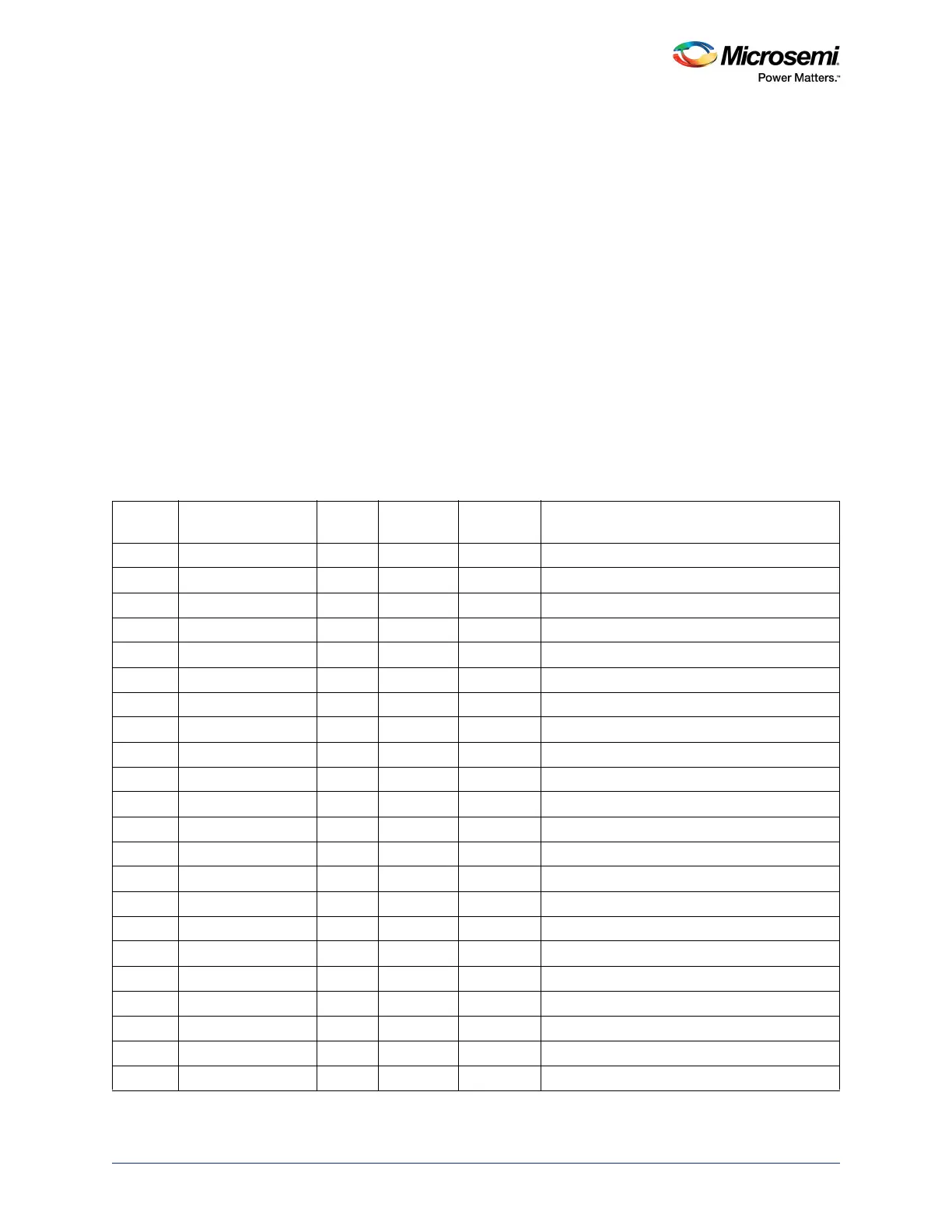
Table 467 • MMUART Register Definitions
Register
Name
Divisor Latch
Access Bit (DLAB)
1
1. DLAB is the MSB of the line control register (LCR bit 7).
Addres
s Offset Read/Write
Reset
Value Description
RBR 0 0x0 R N/A Receiver buffer register
THR 0 0x0 W N/A Transmit holding register
DLR 1 0x0 R/W 0x01 Divisor latch (LSB)
DMR 1 0x04 R/W 0 Divisor latch (MSB)
DFR N/A 0x3C R/W 0 Fractional divisor register
IER 0 0x04 R/W 0 Interrupt enable register
IEM N/A 0x24 R/W 0 Multi-mode interrupt enable register
IIR N/A 0x08 R 0x01 Interrupt identification register
IIM N/A 0x28 Clear on R 0 Multi-mode interrupt identification register
FCR N/A 0x08 W 0 FIFO control register
LCR N/A 0x0C R/W 0 Line control register
MCR N/A 0x10 R/W 0 Modem control register
LSR N/A 0x14 R 0x60 Line status register
MSR N/A 0x18 R 0 Modem status register
SR N/A 0x1C R/W 0 Scratch register
MM0 N/A 0x30 R/W 0 Multi-mode control register0
MM1 N/A 0x34 R/W 0 Multi-mode control register1
MM2 N/A 0x38 R/W 0 Multi-mode control register2
GFR N/A 0x44 R/W 0 Glitch filter register
TTG N/A 0x48 R/W 0 Transmitter time guard register
RTO N/A 0x4C R/W 0 Receiver time-out register
ADR N/A 0x50 R/W 0 Address register