AHB Bus Matrix
UG0331 User Guide Revision 15.0 214
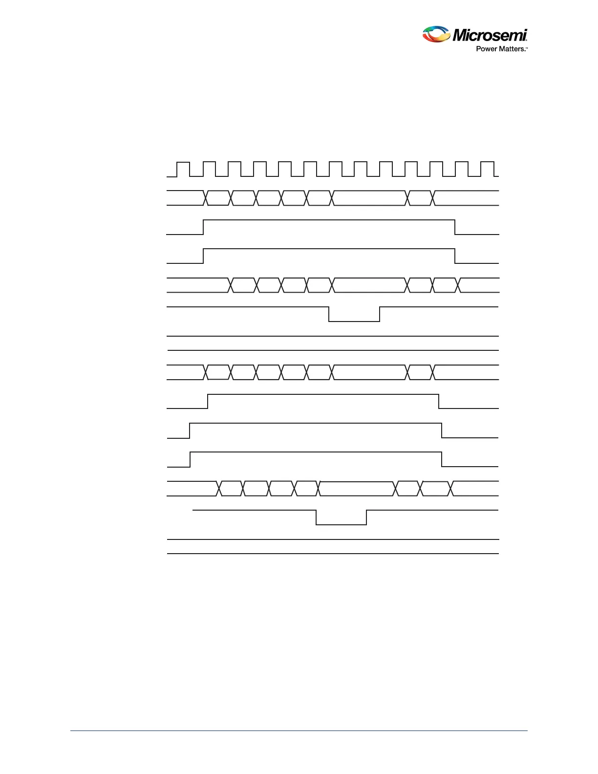
7.1.2 Timing Diagrams
The following figures are the functional timing diagrams for AHBL read/write transactions through the
AHB bus matrix and AHB-to-AHB bridge. Signals to/from a master are denoted by X in the signal name,
and signals to/from a slave are denoted with Y in the signal name. For example, if Cortex-M3 processor
master initiates the transactions of read/write to the eSRAM slave then the signals with X in the signal
name indicates the signals of the Cortex-M3 processor and signals with Y indicate slave eSRAM signals.
Figure 104 • AHB-Lite Write Transactions
HCLK
X_HADDR[31:0]
X_HTRANS
X_HWRITE
X_HWDATA[31:0]
X_HREADY
X_HRESP 0
X_HMASTLOCK 0
Y_HADDR[31:0]
Y_HSEL
Y_HTRANS
Y_HWRITE
Y_HWDATA[31:0]
Y_HREADY
Y_HRESP 0
Y_HMAST 0
AD0
AD0
AD1
AD2 AD3 AD4 AD5 AD6
AD1 AD2 AD3 AD4 AD5 AD6
D0 D1 D3D2 D4 D5 D6
D0 D1 D2 D3 D4 D5 D6