Universal Serial Bus OTG Controller
UG0331 User Guide Revision 15.0 356
Notes:
• Allowed values of x are 1, 2, 3, and 4, corresponding to DMA channels 1 through 4.
• For CH2_DMA_CTRL_REG register the address is 0x40043214.
• For CH3_DMA_CTRL_REG register the address is 0x40043224
• For CH4_DMA_CTRL_REG register the address is 0x40043234.
10.3.12.4 CHx_DMA_ADDR_REG Bit Definitions
Notes:
• Allowed values of x are 1, 2, 3, and 4, corresponding to DMA channels 1 through 4.
• For CH2_DMA_ADDR_REG register the address is 0x40043218.
• For CH3_DMA_ADDR_REG register the address is 0x40043228.
• For CH4_DMA_ADDR_REG register the address is 0x40043238
8 DMA_ERR 0 Bus error bit. Indicates that a bus error has been observed on the input
AHB_HRESPM[1:0] coming from the AHB bus matrix, originating from the
Cortex-M3 processor (or fabric master). This bit is cleared by the software.
[7:4] DMAEP 0 The endpoint number (EP0/EP1/EP2/EP3/EP4) this channel is assigned to.
3 DMAIE 0 DMA interrupt enable
2 DMAMODE 0 Selects DMA Transfer mode.
0: DMA Mode 0 transfer
1: DMA Mode 1 transfer
3 DMA_DIR 0 Selects the DMA transfer direction.
0: DMA write (receive endpoint)
1: DMA read (transmit endpoint)
2 DMA_ENAB 0 Enables the DMA transfer and will cause the transfer to begin.
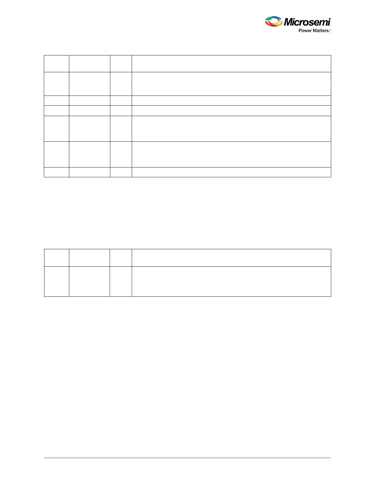
Table 295 • CHx_DMA_ADDR_REG (0x40043208)
Bit
Number Name
Reset
Value Function
[31:0] DMA_ADDR 0 The DMA memory address
The initial memory address written to this register must have a value such that its
modulo 4 value is equal to 0. That is, DMA_ADDR[1:0] must be equal to 00. The
lower two bits of this register are read only and cannot be set by software.
Table 294 • CHx_DMA_CTRL_REG (0x40043204) (continued)
Bit
Number Name
Reset
Value Function