Reset Controller
UG0331 User Guide Revision 15.0 648
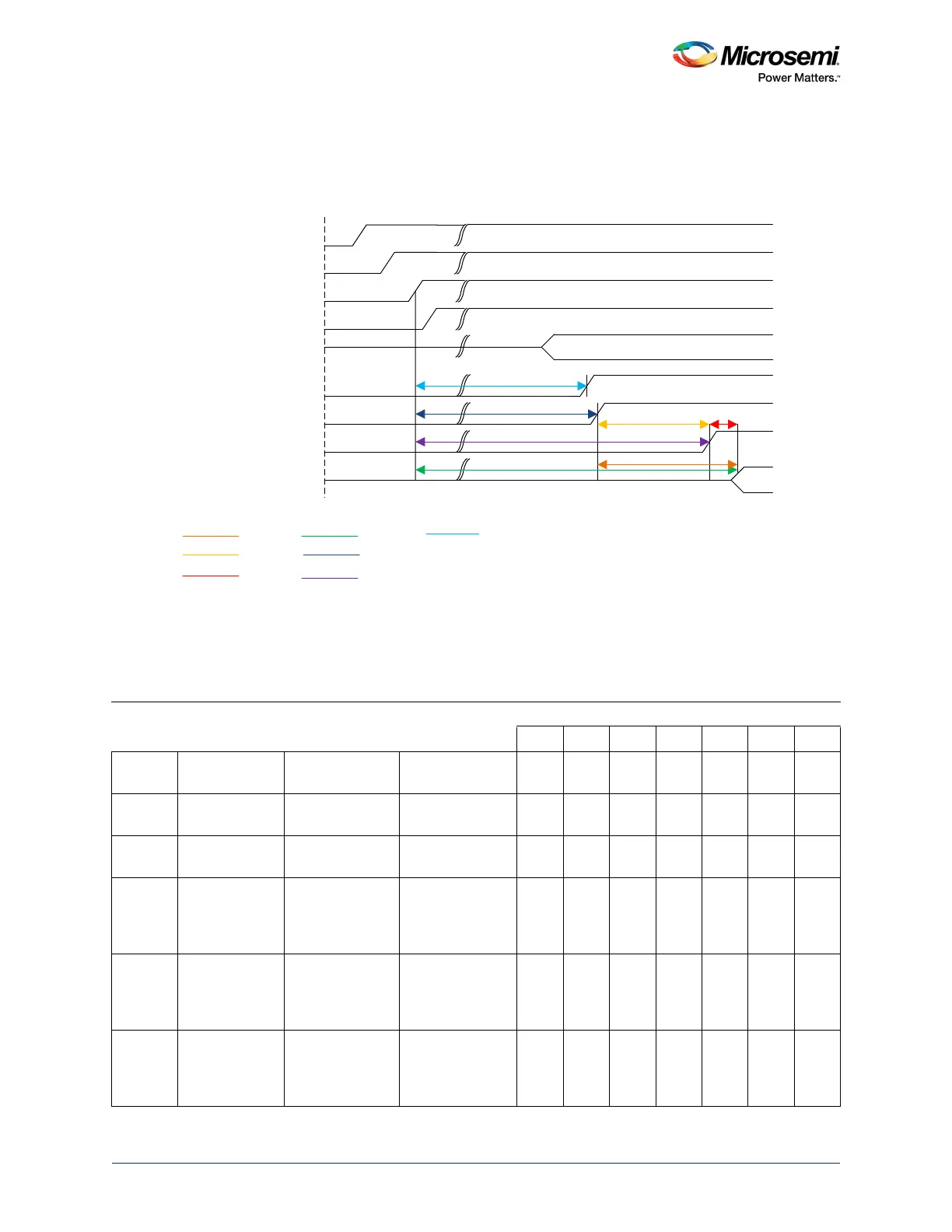
The following figure shows the behavior of different signals when VDD is ramped with a power on reset
delay of 1 ms from 0 V to its minimum threshold level and MSS is used with VDD = 1.2 V, VDDI = 2.5 V,
Tj = 25 °C, and power on reset delay setting = 1 ms.
Figure 281 • VDD Power-up to functional timing diagram
The following table lists power-up to functional time data of M2S005, M2S010, M2S025, M2S050,
M2S060, M2S090, and M2S150 devices with MSS clock ranging from 3 MHz to 166 MHz.
Note: The timing numbers shown in the below table is for worst case condition.
Table 645 • VDD Power-Up to Functional Time
Test
Case Start Point End Point Description
Power-Up to Functional Time (µs)
005 010 025 050 060 090 150
Case1 POWER_ON_R
ESET_N
Output available
at I/O
Fabric to output 647 500 531 483 474 524 647
Case 2 POWER_ON_R
ESET_N
MSS_RESET_N
_ M2F
Fabric to MSS 644 497 528 480 468 518 641
Case 3 MSS_RESET_
N_M2F
Output available
at I/O
MSS to output 3.6 3.6 3.6 3.4 4.9 4.8 4.8
Case 4
V
DD Output available
at I/O
V
DD
at its
minimum
threshold level to
output
3096 2975 3012 2959 2869 2992 3225
Case 5
V
DD POWER_ON_
RESET_N
V
DD
at its
minimum
threshold level to
fabric
2476 2487 2496 2486 2406 2563 2602
Case 6
V
DD MSS_RESET_N
_ M2F
V
DD
at its
minimum
threshold level to
MSS
3093 2972 3008 2956 2864 2987 3220
'(9567B1
9339'',[
9
''
,1%8)
,1%8):($.38//
06,206,2'''5,2
32:(5B21B5(6(7B1
066B5(6(7B1B0)
287%8)
PV
PV
PV
PV
V
V
V
5&26&B0+]
06
&DVH
&DVH
&DVH
&DVH
&DVH
&DVH
+LJK=
+LJK=
7ULVWDWH
7ULVWDWH
&DVH