Reset Controller
UG0331 User Guide Revision 15.0 649
Note: Time taken for different power-on reset delay settings can be calculated using the following equation:
(Test case – 2000 µs) + 2 × Power on Reset Delay setting.
Case 7
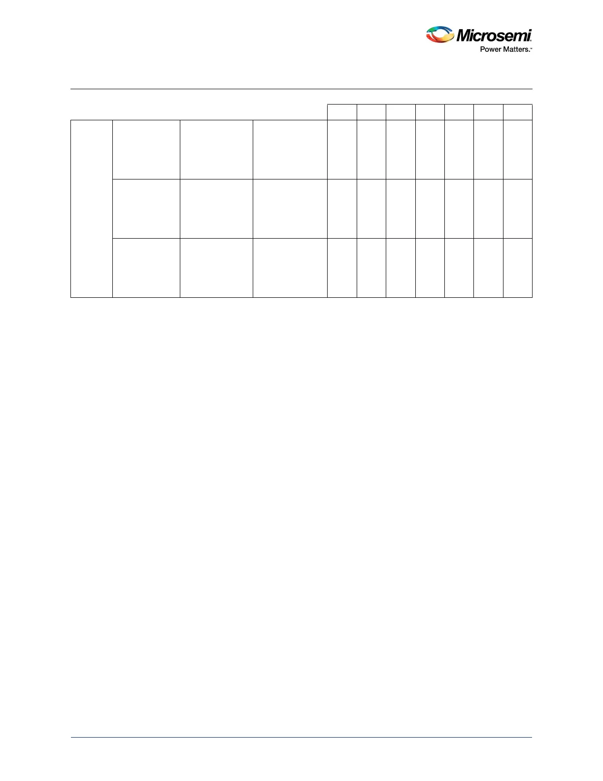
V
DD
DDRIO input
buffer weak pull
V
DD
at its
minimum
threshold level to
input buffer weak
pull
2500 2487 2509 2475 2507 2519 2617
V
DD
MSIO i nput b u ffe r
weak pull
V
DD
at its
minimum
threshold level to
input buffer weak
pull
2504 2491 2510 2478 2517 2525 2620
V
DD
MSIOD input
buffer weak pull
V
DD
at its
minimum
threshold level to
input buffer weak
pull
2479 2468 2493 2458 2486 2499 2595
Table 645 • VDD Power-Up to Functional Time (continued)
Test
Case Start Point End Point Description
Power-Up to Functional Time (µs)
005 010 025 050 060 090 150