Inter-Integrated Circuit Peripherals
UG0331 User Guide Revision 15.0 551
15.4.1 Control Register
The following table describes the Control register used for configuring the I
2
C peripherals.
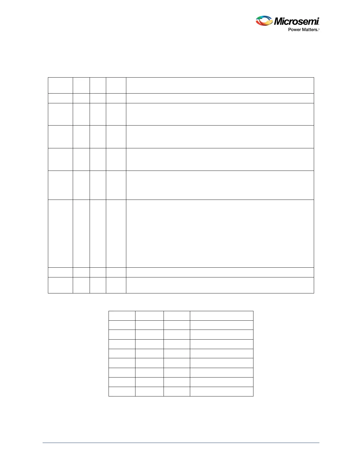
Table 521 • Control Register (CTRL)
Bit
Number Name R/W
Reset
Value Description
7 CR2 R/W 0 Clock rate bit 2; refer to bit 0.
6 ENS1 R/W 0 Enable bit. When ENS1 = 0, the SDA and SCL outputs are in a high impedance
and SDA and SCL input signals are ignored. When ENS1 = 1, the I
2
C is
enabled.
5 STA R/W 0 The Start flag. When STA = 1, the I
2
C peripheral checks the status of the serial
bus and generates a START condition, if the bus is free. STA bit is
automatically cleared after START condition has been generated.
4 STO R/W 0 The Stop flag. When STO = 1 and the I
2
C is in Master mode, a STOP condition
is transmitted to the serial bus. STO bit is automatically cleared after STOP
condition has been generated.
3 SI R/W 0 The SI flag. The SI flag is set by the I
2
C whenever there is a serviceable
change in the Status register. Once the register is updated, the SI bit must be
cleared by software.
The SI bit is directly readable through the APB INTERRUPT signal.
2 AA R/W 0 The assert acknowledge flag.
When AA = 1, an acknowledge is returned when:
– The own slave address is received
– The general call address is received when the GC bit in the address register
is set
– A data byte is received when the core is in the Master-receiver mode
– A data byte is received when the core is in the Slave-receiver mode.
When AA = 0, a not acknowledge is returned when:
– A data byte is received while the core is in Master-receiver mode
– A data byte is received when I
2
C peripheral is in Slave-receiver mode
1 CR1 R/W 0 Serial clock rate bit 1; refer to bit 0
0 CR0 R/W 0 Serial clock rate bit 0. Clock rate is defined in Table 522, page 551.
BCLK is synchronized to PCLK and hence must be PCLKFREQ/2 or less.
Table 522 • Clock Rate (CR)
CR2 CR1 CR0 SCL Frequency
0 0 0 PCLK frequency/256
0 0 1 PCLK frequency/224
0 1 0 PCLK frequency/192
0 1 1 PCLK frequency/160
1 0 0 PCLK frequency/960
1 0 1 PCLK frequency/120
1 1 0 PCLK frequency/60
1 1 1 BCLK frequency/8