Cortex-M3 Processor Overview and Debug Features
UG0331 User Guide Revision 15.0 14
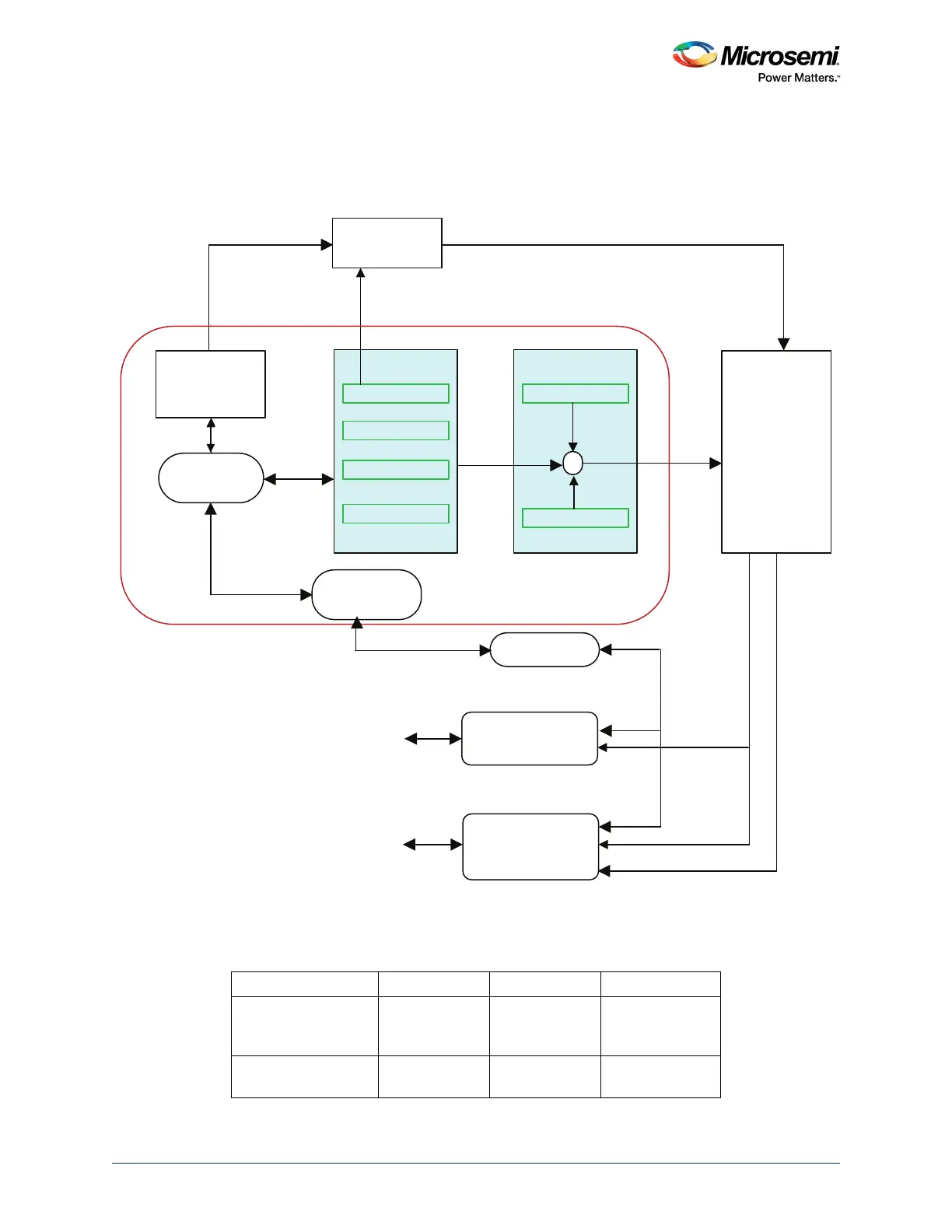
The following figure shows the diagram of a Cortex-M3 processor trace system. JTAG/SWD, SWO, and
the 4-bit parallel trace port can be deployed into a 20-pin Cortex Debug + ETM connector on the target.
Note: The TDO signal of JTAG is multiplexed with SWO, so that SWO trace is not accessible when the DP is in
a JTAG configuration. Only the SWD interface can be used together with SWO.
Figure 2 • Trace System Block Diagram
The following table shows pin multiplexing details for JTAG, SWD, and ETM modes of the debug section.
For more details on pin information, refer to the DS0115: SmartFusion2 Pin Descriptions Datasheet.
Table 3 • Signal Multiplexing
FPGA Pin JTAG Mode SWD Mode ETM Mode
JTAG_TMS/
M3_TMS/
M3_SWDIO
TMS SWDIO SWDIO
JTAG_TCK/
M3_TCK
TCK SWCLK SWCLK
Cortex-M 3
Processor Core
AHB Bus
Matrix
ETM
DWT
PC Sampler
Interrupt Trace
4 Watch points
ETM Trigger
ITM
Time Stamp
Software Trace
Trace Port
Interface Unit
(TPIU)
AHB -AP
DP
Cortex-M3 Processor
Debug (Serial Wire
or JTAG)
Trigger
ATB
ATB
ATB
ATB
System
Bus
DAP BUS
SWO
4-Bit
Trace
JTAG /
SWD
To Standard JTAG
Connector via IO
pads
To Trace for Cortex-M3 Processor
Connector via
FPGA Fabric
CPU I/F
Cortex- M3 Processor
Cortex-M3 Processor
Debug + EMT