MSS GPIO
UG0331 User Guide Revision 15.0 565
16.2.1 MSS GPIO Configuration Registers (GPIO_X_CFG)
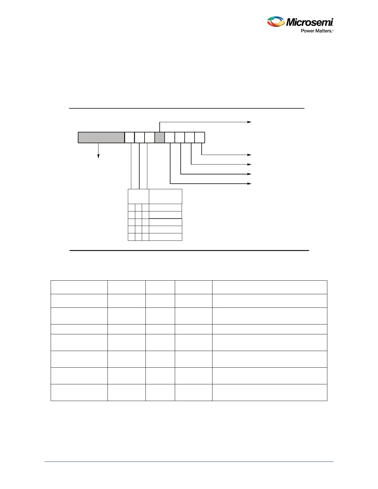
In the MSS GPIO block, each GPIO has a 32-bit configuration register. The configuration register allows
selection of the GPIO in Input, Output, or Bi-directional mode. A GPIO can also be used as an interrupt
when it is configured in Bi-directional mode. The offset address of MSS GPIO block configuration
registers is given in Ta ble 5 38, page 574. The following figure shows the detailed configuration register
bit definitions.
Figure 242 • GPIO Configuration Register (GPIO_X_CFG)
The following table provides bit definitions for the GPIO configuration registers.
Table 535 • GPIO_X_CFG
Bit Number Name Type Reset Value Description
GPIO_X_CFG[31:8] Reserved R/W 0h000000 Reserved
GPIO_X_CFG[7:5] TYPES_INT_I R/W 0b000 Input interrupt type configuration
Refer Figure 242, page 565 for Bit definitions.
GPIO_X_CFG[4] Reserved R/W 0b0 Reserved
GPIO_X_CFG[3] EN_INT_i R/W 0b0 0: Interrupt disabled
1: Interrupt enabled
GPIO_X_CFG[2] GPIO_i_OE R/W 0b0 0: Disable output buffer
1: Enable output buffer
GPIO_X_CFG[1] EN_IN_i R/W 0b0 0: Input register disabled
1: Input register enabled
GPIO_X_CFG[0] EN_OUT_i R/W 0b0 0: Output register disabled
1: Output register enabled
Not Used
31:8
7
6
5
4
3
2
1
0
Not Used
Output Reg Enable
Input Reg Enable
Output Buffer Enable
Interrupt Enable
Edge Both
Interrupt
Type
000
00
1
010
0
1
1
0
0
1
Edge Negative
Edge Positive
Level Low
Level High
Bit
Definitions
CONFIG_X (X = 0 to 31)