Universal Serial Bus OTG Controller
UG0331 User Guide Revision 15.0 332
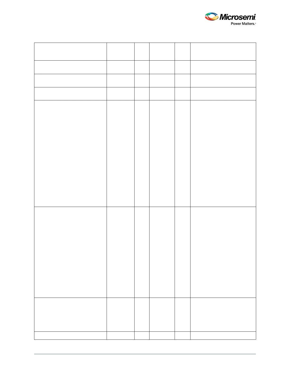
RX_FIFO_SIZE_REG (0x40043063) 0x0063 5 RW 0 Controls the size of the selected
receive endpoint FIFO.
TX_FIFO_ADD_REG (0x40043064) 0x0064 14 RW 0 Controls the start address of the
selected transmit endpoint FIFO.
RX_FIFO_ADD_REG (0x40043066) 0x0066 14 RW 0 Controls the start address of the
selected receive endpoint FIFO.
VBUS_CSR_REG (write only)
(0x40043068)
0x0068 4 W
(VControl)
0 VControl is optionally a UTMI+
PHY vendor register. UTMI+
specification defines a 4-bit
VControl register.
The latency for the write (as
measured between the positive
edge of the CLK at the end of the
AHB write cycle and the positive
edge of XCLK when the UTMI+
PHY VControl register is loaded)
will be between Hc + 3Xc and Hc
+ 4Xc, where Hc is a cycle of CLK
and Xc is a cycle of XCLK.
The minimum period between
successive writes to the VControl
register must therefore be Hc +
4Xc to ensure that the value is not
corrupted while it is being
synchronized to the XCLK
domain.
VBUS_CSR_REG (read only)
(0x40043068)
0x0068 8 R
(VStatus)
VStatus is optionally a UTMI+
PHY vendor register. UTMI+
specification defines an 8-bit
VStatus register.
The VSTATUS input bus is
sampled once every 6 XCLK
cycles.
The latency between the
VSTATUS input bus from the PHY
changing and the new value
being read from the VStatus
register (measured to the positive
edge of CLK at the end of the
AHB read cycle) will be between
2Hc + Xc and 3Hc + 6Xc, where
Hc is a cycle of CLK and Xc is a
cycle of XCLK.
HW_VERSION_REG (0x4004306C) 0x006C 16 R Returns information about the
version of the USB controller.
Specifically, the version of design
(RTL) used to implement the USB
controller. Useful for debug
purposes.
Reserved 0x006E N/A
Table 240 • Additional Control and Status Registers (OTG, Dynamic FIFO, and Version) (continued)
Register Name
Address
Offset from
0x40043000 Width R/W Type
Reset
Value Description